Method for improving exposure uniformity of PCB

A technology of PCB board and uniformity, applied in the field of improving the exposure uniformity of PCB board, can solve the problems of over-exposure or false exposure, affecting product quality, uneven board thickness, etc., and achieve the effect of high-precision measurement

Active Publication Date: 2022-07-05
圆周率半导体(南通)有限公司
View PDF8 Cites 0 Cited by
  • Summary
  • Abstract
  • Description
  • Claims
  • Application Information

AI Technical Summary

Problems solved by technology

However, the existing PCB board may have the problem of uneven board thickness. When the PCB board thickness is uneven, the exposure energy received by the PCB board surface is inconsistent, and the risk of local overexposure or virtual exposure is likely to occur, resulting in open circuit or loss of circuit. Membrane is not clean, serious will affect the quality of the product

Method used


Image

  • Method for improving exposure uniformity of PCB
  • Method for improving exposure uniformity of PCB

Examples


Embodiment 1

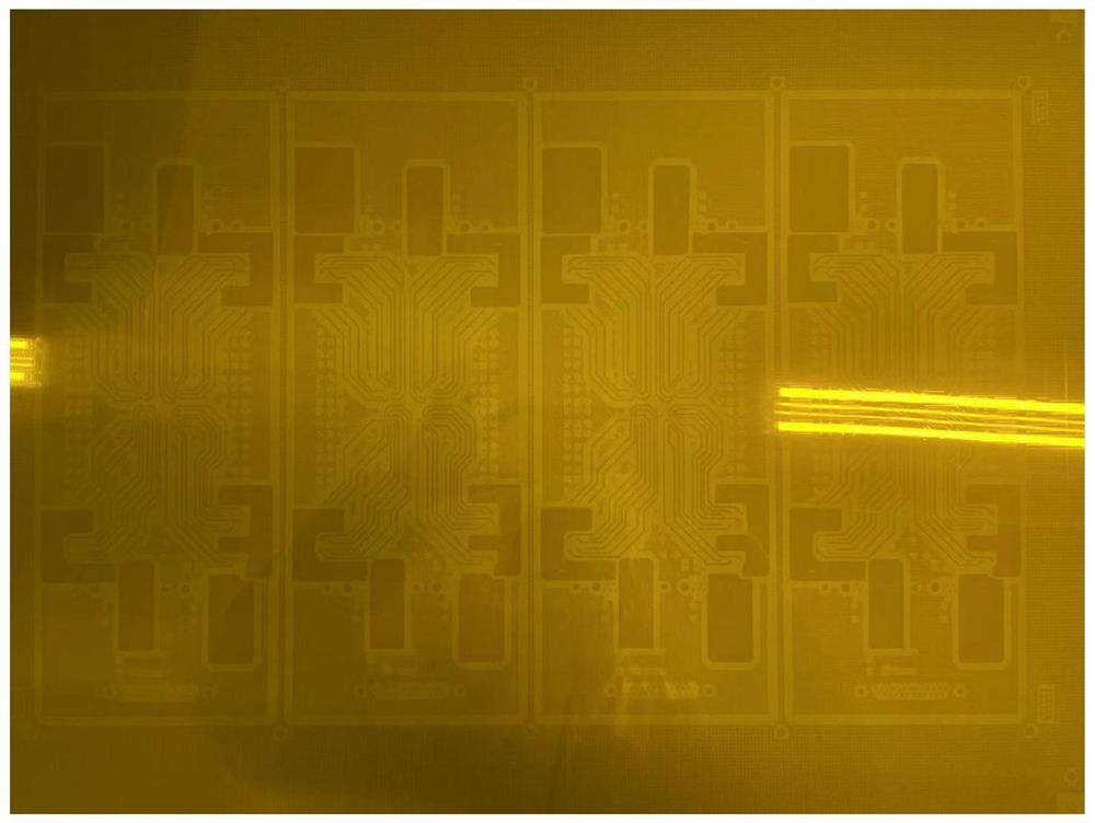
[0027] Taking a product A as an example, the theoretical design thickness of this product is 210mil, the size is 18*24inch, the tolerance control of the customer's board thickness is + / -7%, and the control of the residual copper in deep drilling is 2-10mil. This product operates a total of 6WPNL , the thickness of the board is measured after lamination and milling.

[0028] Put this board into the measuring table one by one, use the chuck to clamp the product, start the equipment and start working, the set measuring grid is 1*1mm, the thickness of the entire board needs to be measured, and this measurement is based on the configuration of the equipment. 278,709 points are required to complete the coverage of the entire surface. The measurement speed of the equipment is 500 times / s, so the measurement time of the entire board surface is 9 minutes. The specific steps are as follows:

[0029] 1. After the PCB to be tested is fixed by the fixture, the laser Mark head starts first,...


PUM

PropertyMeasurementUnit
thicknessaaaaaaaaaa

Abstract

The invention provides a method for improving exposure uniformity of a PCB (Printed Circuit Board). The method comprises the following steps of: obtaining a theoretical thickness value of the PCB; measuring the thickness of each grid on the PCB; the difference value of each grid is imported into a data model established by modeling software from top to bottom and from left to right, and is visually displayed by adopting different colors; mask plates are prepared, each mask plate comprises a light-transmitting area and a light-proof area, and the light-transmitting area of each mask plate is matched with the area corresponding to the single color; the mask plates are adopted to expose the PCB one by one, the focal length of the exposure machine is adjusted according to different colors corresponding to the mask plates, and the exposure machine projects light penetrating through the light-transmitting area to the PCB for pattern transfer. The plate thickness distribution diagram can express the plate thickness distribution of the plate surface and the region, so that focal length adjustment of regional exposure during exposure is guided, exposure energy received by the whole plate surface is consistent, the risk of local overexposure or exposure deficiency is avoided, and the problem of circuit open circuit or incomplete film removal caused by inconsistent exposure energy is solved.

Description

technical field [0001] The invention relates to the technical field of printed circuits, in particular to a method for improving the exposure uniformity of a PCB board. Background technique [0002] Exposure is a very important part in the production process of the PCB board, and its main purpose is to transfer the image on the original film to the photosensitive base plate through the action of the light source. Since exposure is a process in which ultraviolet light is transmitted through a film negative to cause photopolymerization of the photoresist material, it is required that the exposure energy must be uniform. The existing PCB board may have the problem of uneven thickness. When the thickness of the PCB is uneven, the exposure energy received by the PCB surface is inconsistent, which is prone to the risk of local overexposure or virtual exposure, resulting in open circuits or faults. The defect of the membrane is not clean, which will seriously affect the quality of...

Claims


Application Information

Patent Timeline
Patent Type & Authority Applications(China)
IPC IPC(8): G03F7/20
CPCG03F7/70508G03F7/7055
Inventor 吴鹏何静安龙能水陈定康盛从学章恒
Owner 圆周率半导体(南通)有限公司
Why Eureka
Try Eureka