Silicon optical chip design method capable of automatically controlling temperature

A silicon photonics chip and design method technology, applied in temperature control, control/regulation system, non-electric variable control, etc., can solve the problems of reduced yield rate of silicon photonics chip, increased cost, and reduced advantages of high integration of silicon photonics chip , to achieve the effect of cost reduction, reduction of defective rate, and reduction of control components

Pending Publication Date: 2022-07-15
SUZHOU CREALIGHTS TECH
View PDF0 Cites 0 Cited by
  • Summary
  • Abstract
  • Description
  • Claims
  • Application Information

AI Technical Summary

Problems solved by technology

In this way, due to the increase of external control components, the advantage of high integration of the silicon photonic chip itself is reduced; at the same time, due to the increase in the number of silicon photonic MPDs, the overall silicon photonic chip yield rate is reduced, resulting in an increase in cost

Method used


Image

  • Silicon optical chip design method capable of automatically controlling temperature
  • Silicon optical chip design method capable of automatically controlling temperature
  • Silicon optical chip design method capable of automatically controlling temperature

Examples


Embodiment 1

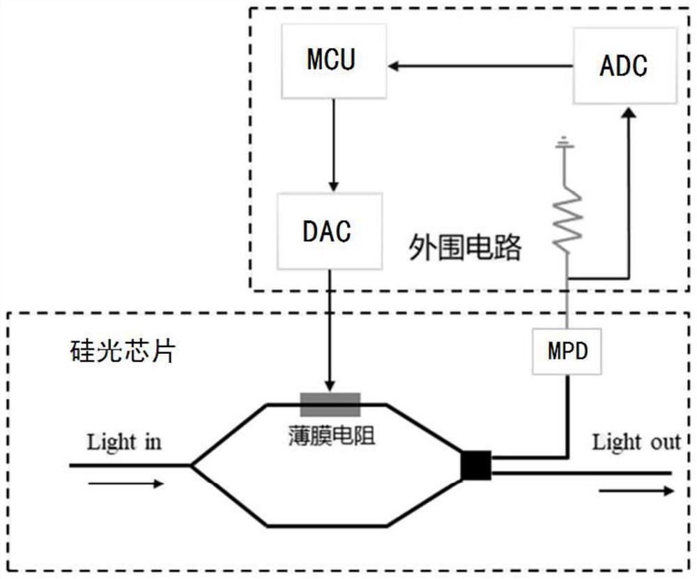
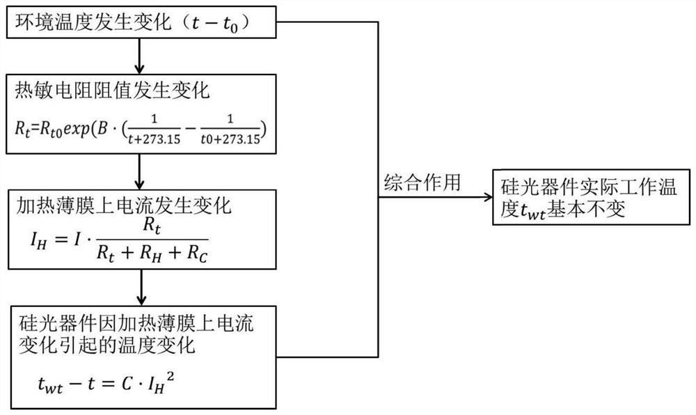
[0060] like image 3 As shown in the figure, a thin film heating resistor is deposited above the silicon photonics device inside the chip, and a fixed-value resistor is connected in series inside the chip and then connected in parallel with the thermistor, which is exported to the pad on the PCB through the gold wire, and is connected to the constant current power chip. The other end is grounded, which refers to the negative electrode of the constant current power supply chip. Usually, the negative electrode of the constant current power supply chip is the same end as the ground end of the entire PCB. In this embodiment, the thermistor is arranged on the silicon photonics chip, and the connection and fixation of the thermistor is realized by arranging pads on the silicon photonics chip, and then the two ends of the thermistor are respectively connected with the constant current power supply chip. Two-pole connection.

Embodiment 2

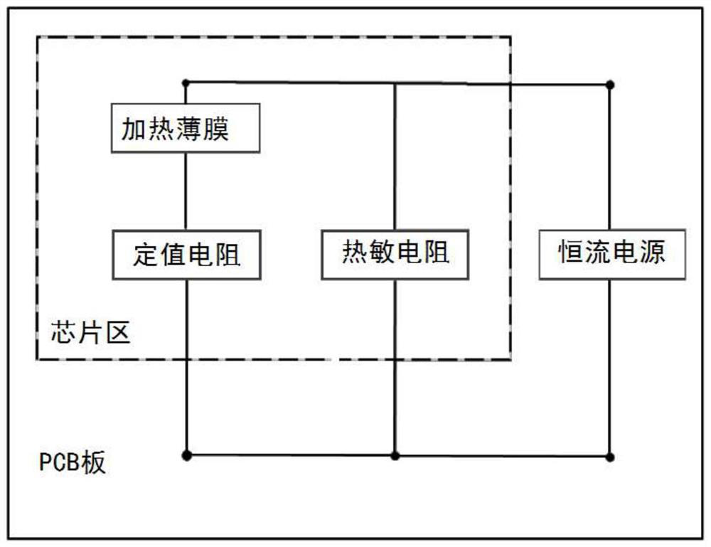
[0062] like Figure 4 As shown, the same as Embodiment 1, the difference is that the resistor connected in series with the thin film heating resistor is welded on the PCB outside the chip, and is connected to the chip area through a gold wire, and the resistor can be adjusted according to the situation. Figure 4 Among them, 1 is a chip, 2 is a film heating resistor, 3 is a thermistor, 4 is an adjustable resistor, 5 is a constant current power supply, and 6 is a PCB board.

[0063] The feasibility of the above embodiments is analyzed below.

[0064] Taking the silicon photonics Mach-Zehnder Interferometer (MZI) as an example for analysis, this structure is widely used in various silicon photonics devices, including modulators, filters, optical switches, attenuators and so on.

[0065] For a silicon-optical MZI interferometer, the transfer function is:

[0066] I 0 / I i =0.5×[1+cos(βΔL)]

[0067] Among them, β=2πn eff / λ is the propagation constant of the silicon optical ...


PUM


Abstract

The invention provides a design method of a silicon optical chip with an autonomous temperature control function, relates to the technical field of silicon optical chips, and aims to easily convert an original complicated silicon optical chip temperature control system into a simple passive autonomous temperature control system by using a very simple parallel circuit system, reduce additional elements and reduce the reject ratio of chips. According to the design method, a thermistor is additionally arranged on a silicon optical chip, so that the thermistor is connected with a thin-film resistor of the silicon optical chip in parallel to form a parallel circuit, and fixed current is input into the parallel circuit; according to the phenomenon that the resistance value of the thermistor is changed along with the temperature change so as to change the current of the thermistor branch, the current regulation of the thin-film resistor branch is realized, and the autonomous temperature control of the silicon optical chip is further realized; the thermistor is a thermistor with a negative temperature coefficient, and the thin-film resistor is a thin-film heating resistor.

Description

technical field [0001] The invention relates to the technical field of silicon photonics chips, in particular to a silicon photonics chip design method with independent temperature control. Background technique [0002] With the development of optical communication networks in the direction of integration, low power consumption, intelligence and large capacity, silicon photonics technology in high-speed optical chips has the advantages of low cost, high integration, large bandwidth, etc. The requirements of network resources are one of the main technologies actively deployed and developed by major manufacturers around the world. However, due to the high thermo-optic coefficient of silicon material, silicon optical devices will change the refractive index of light with the change of temperature, and then cause the change of the transmittance of the device. This requires a temperature control device to be added to the silicon optical device itself to adjust the transmittance ...

Claims


Application Information

Patent Timeline
IPC IPC(8): G05D23/24
CPCG05D23/24
Inventor 赵波林天营孙旭胡朝阳
Owner SUZHOU CREALIGHTS TECH
Why Eureka
Try Eureka