
Voltage buffer circuit

A voltage buffering and circuit technology, applied in the field of image sensors, can solve problems such as long voltage stabilization time and failure to reach the working sequence

Pending Publication Date: 2022-07-15
CHENGDU LIGHT COLLECTOR TECH
View PDF1 Cites 0 Cited by
  • Summary
  • Abstract
  • Description
  • Claims
  • Application Information

AI Technical Summary

Problems solved by technology

Under static operation, the gate of the MOS transistor is generally considered to be approximately a capacitive load, and no current passes through it. Therefore, the voltage buffer circuit used as the reference voltage input and output can use a conventional structure double-ended input and single-ended output error amplifier, but If in some functional requirements, the reference voltage needs to be switched according to the working sequence, that is to say, the gate potential of the MOS transistor as the receiving end changes in the time domain, then a charging and discharging current will be generated on the gate, so that the reference The potential of the voltage will need a stabilization process
If the number of MOS devices receiving the reference voltage is small, the conventional voltage buffer circuit can still meet the application requirements, but if a large number of MOS device gates are connected to the output terminal of a voltage buffer circuit at the same time, the transmitted voltage is constantly switching. , the voltage buffer circuit will have insufficient drive, and the voltage stabilization time is too long to meet the requirements of the working sequence, which limits the length of the working sequence

Method used


Image

  • Voltage buffer circuit
  • Voltage buffer circuit
  • Voltage buffer circuit

Examples


Embodiment Construction

[0043] The specific embodiments of the present invention will be described in more detail below with reference to the schematic diagrams. The advantages and features of the present invention will become more apparent from the following description. It should be noted that the accompanying drawings are all in a very simplified form and in inaccurate scales, and are only used to facilitate and clearly assist the purpose of explaining the embodiments of the present invention.

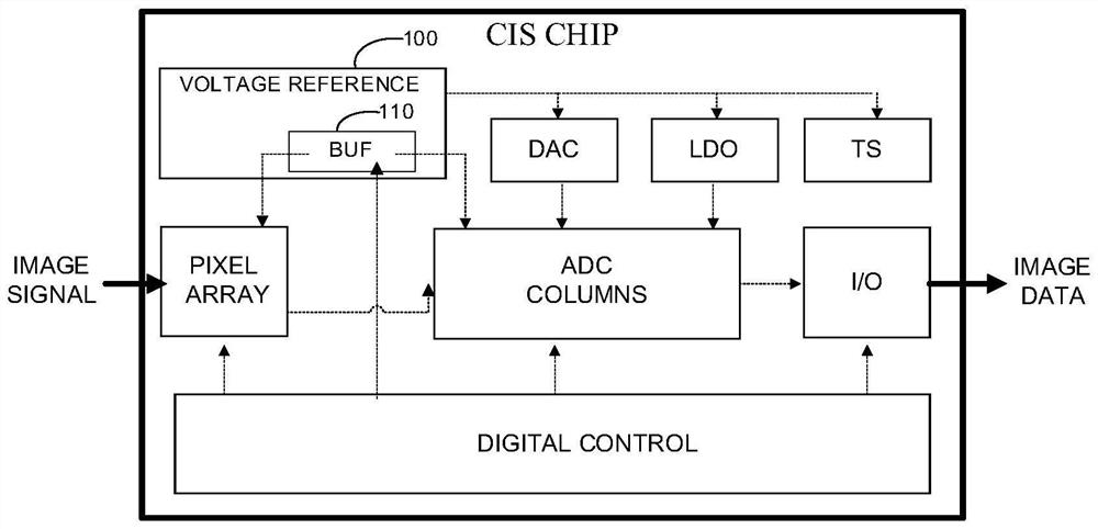
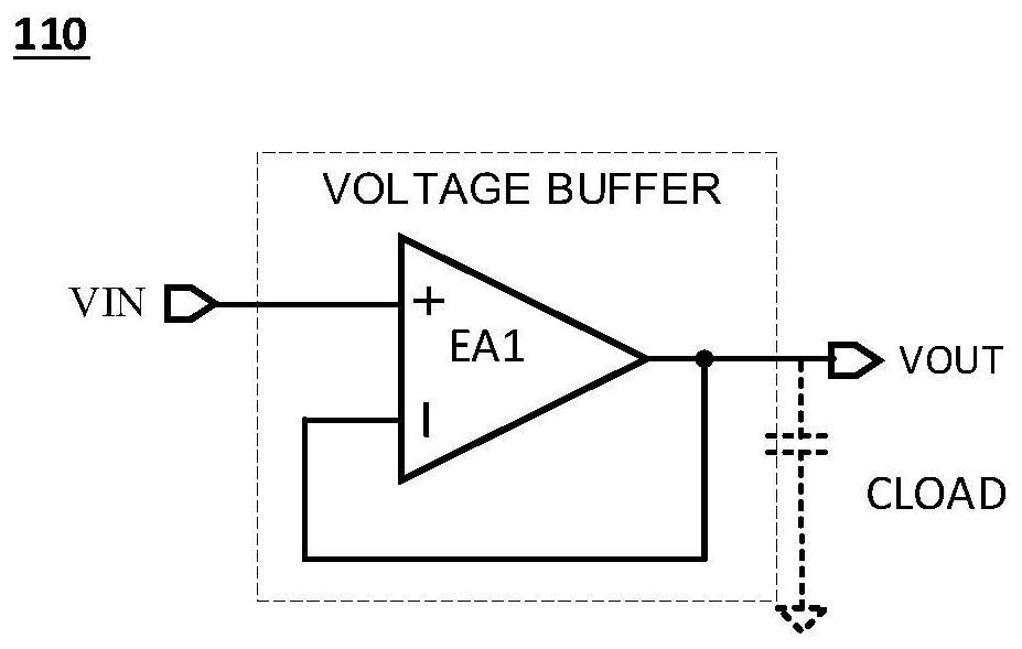
[0044] figure 1 It is a schematic diagram of the application environment of the reference voltage in a CMOS image sensor system. like figure 1 As shown, the reference voltage source 100 provides a reference voltage for other various circuit modules, and the voltage value of the reference voltage generally needs to be stable and does not change with changes in the external environment. The output voltage of the reference voltage source 110 itself has no driving capability, and if it is directly transmitt...


PUM


Abstract

The invention provides a voltage buffer circuit, an input module comprises a first differential amplifier and a second differential amplifier which are used for receiving input voltage, and the output end of the first differential amplifier and the output end of the second differential amplifier respectively output a first potential signal and a second potential signal. The output module comprises a driving output unit, the driving output unit is provided with a first driving MOS tube and a second driving MOS tube, and the output module adjusts driving currents of the first driving MOS tube and the second driving MOS tube according to the first potential signal and the second potential signal. And the voltage of the output end VOUT of the voltage buffer circuit follows the input voltage VIN. The first differential amplifier is used for receiving the higher range input voltage, and the second differential amplifier is used for receiving the lower range input voltage, so that the voltage buffer circuit can receive the full range input voltage. The output module can provide a large instantaneous current to charge and discharge a load.

Description

technical field [0001] The present invention relates to the technical field of image sensors, in particular to a voltage buffer circuit. Background technique [0002] CMOS image sensor chips have been continuously developed in recent years, and have gradually replaced CCDs and are widely used in various portable imaging electronic equipment, security monitoring equipment, vehicle electronics, etc. As an important performance index, high frame rate directly affects the dynamic imaging quality and becomes one of the most concerned issues for designers. [0003] Many circuit modules in a CMOS image sensor are used to achieve different functions. In each functional module in the circuit module, the reference voltage source module needs to provide a reference voltage during normal operation, and most of the output reference voltages are supplied to the gate of the MOS tube. Under static operation, the gate of the MOS tube is generally considered to be a capacitive load and does...

Claims


Application Information

Patent Timeline
IPC IPC(8): G05F1/56
CPCG05F1/56Y02B70/10
Inventor 芮松鹏蔡化王勇陈飞魏聪高菊
Owner CHENGDU LIGHT COLLECTOR TECH
Learn More