Manufacturing method of quantum well optical detector and quantum well optical detector

A technology of optical detectors and manufacturing methods, which can be applied to semiconductor devices, electrical components, circuits, etc., and can solve the problems of low short-wave infrared responsivity

Pending Publication Date: 2022-07-15
GUANGDONG GREATER BAY AREA INST OF INTEGRATED CIRCUIT & SYST +1
View PDF9 Cites 0 Cited by
  • Summary
  • Abstract
  • Description
  • Claims
  • Application Information

AI Technical Summary

Problems solved by technology

[0005] The main purpose of this application is to provide a method for making a quantum well photodetector and a quantum well photodetector to solve the problem of low responsivity of Ge material photodetectors to short-wave infrared in the prior art

Method used


Image

  • Manufacturing method of quantum well optical detector and quantum well optical detector
  • Manufacturing method of quantum well optical detector and quantum well optical detector
  • Manufacturing method of quantum well optical detector and quantum well optical detector

Examples


Embodiment

[0068] The fabrication method of the quantum well photodetector in this embodiment includes the following processes:

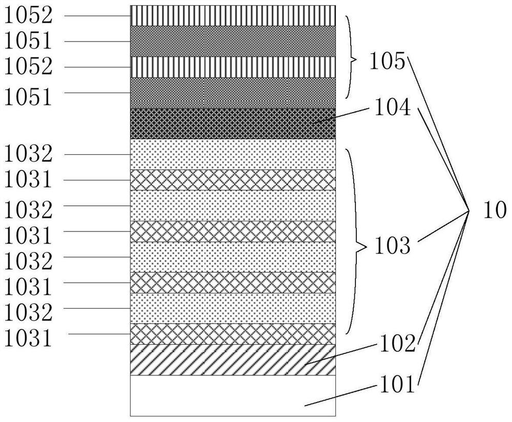
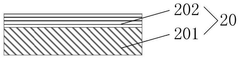
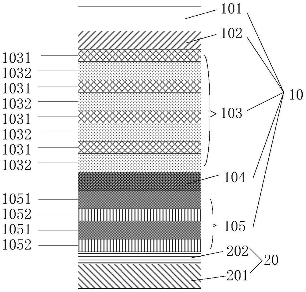
[0069] like Figure 5 As shown, the acceptor substrate 10 is provided, and the acceptor substrate 10 includes a first substrate layer 101, a second Ge buffer layer 107, a first Ge buffer layer 102, a Ge buffer layer 107 and a Ge x Si 1-x / Ge multiple quantum well layer 103, P-type Ge layer 104 and cavity structure 105, the above-mentioned Ge x Si 1-x / Ge multiple quantum well layer 103 includes alternately arranged Ge x Si 1-x Layer 1031 and Ge layer 1032, wherein x is greater than 0.75 and less than or equal to 1, and the above resonant cavity structure 105 includes alternately arranged silicide material layers 1051 and first Al 2 O 3 layer 1052;

[0070] The first substrate layer, the first Ge buffer layer, and the Ge are prepared by a rapid thermal chemical vapor deposition method x Si 1-x The / Ge multiple quantum well layer and the above-mentioned...


PUM

PropertyMeasurementUnit
thicknessaaaaaaaaaa
thicknessaaaaaaaaaa
thicknessaaaaaaaaaa

Abstract

The invention provides a manufacturing method of a quantum well optical detector and the quantum well optical detector, and the method comprises the steps: providing an acceptor substrate which comprises a first substrate layer, a first Ge buffer layer, a GexSi1-x / Ge multi-quantum well layer, a P-type Ge layer and a resonant cavity structure which is alternately provided with silicide material layers and first Al2O3 layers, and the first substrate layer, the first Ge buffer layer, the GexSi1-x / Ge multi-quantum well layer and the P-type Ge layer are stacked in sequence; providing a donor substrate, wherein the donor substrate comprises a second substrate layer and a second Al2O3 layer which are stacked in sequence; bonding the acceptor substrate and the donor substrate; removing the first substrate layer; and injecting ions into the first Ge buffer layer to form an N-type Ge layer. According to the method, by arranging the resonant cavity structure, an optical resonant cavity can be formed in the device, the optical resonant cavity effect is enhanced, and the problem that in the prior art, a Ge material optical detector is low in responsivity to short wave infrared is solved.

Description

technical field [0001] The present application relates to the field of semiconductor detector integration, in particular, to a manufacturing method of a quantum well photodetector and a quantum well photodetector. Background technique [0002] The traditional Ge material photoelectric can realize the detection at the wavelength of 1550nm, but it is limited by the characteristics of the Ge material (the absorption edge of the direct band gap of Ge is 1549nm), 1550nm is close to the detection cut-off wavelength of the Ge material, and the absorption coefficient of the Ge material at the wavelength of 1550nm is small , it is difficult to achieve high responsivity detection of short-wave infrared. The low absorption coefficient can no longer satisfy the efficient detection of short infrared waves, which greatly limits the development of Si-based high-efficiency infrared detection devices. [0003] Therefore, there is an urgent need for a Ge material photodetector with high resp...

Claims


Application Information

Patent Timeline
Patent Type & Authority Applications(China)
IPC IPC(8): H01L31/0352H01L31/028H01L31/0312H01L31/102H01L31/18
CPCH01L31/035236H01L31/028H01L31/0312H01L31/102H01L31/1804
Inventor 亨利·H·阿达姆松谭鑫广赵雪薇孔真真
Owner GUANGDONG GREATER BAY AREA INST OF INTEGRATED CIRCUIT & SYST
Why Eureka
Try Eureka