LPDDR wafer RDL design method suitable for multi-chip failure analysis

A technology of failure analysis and design method, applied in semiconductor/solid-state device components, semiconductor/solid-state device testing/measurement, semiconductor devices, etc., can solve problems such as indistinguishable, time-consuming, and difficult processes

Pending Publication Date: 2022-07-22
PAYTON TECHNOLOGY (SHENZHEN) CO LTD
View PDF0 Cites 0 Cited by
  • Summary
  • Abstract
  • Description
  • Claims
  • Application Information

AI Technical Summary

Problems solved by technology

The process of multi-layer stacking is relatively difficult, and it is prone to the problem of failure caused by cracking of a single DIE
[0003] In the existing technical solutions, there are often multiple (2 to 8) DIEs with a thickness of only 200um to 40um stacked vertically inside an LPDDR package chip. Once a certain DIE cracks and fails, conventional testing machines cannot tell which one it is. If there is a problem with DIE, it is necessary to use a special test machine and a special program for testing to distinguish which chip is abnormal, and it is also necessary to develop a special program for analysis
[0004] The failure analysis of multi-layer packaging products requires the use of special testing machines and special programs to test which chip is abnormal. This kind of special machine is expensive, and special programs need to be specially developed for analysis, and it takes a long time. The cost of use is too high, which affects the cost and efficiency of failure analysis

Method used


Image

  • LPDDR wafer RDL design method suitable for multi-chip failure analysis
  • LPDDR wafer RDL design method suitable for multi-chip failure analysis
  • LPDDR wafer RDL design method suitable for multi-chip failure analysis

Examples


Embodiment Construction

[0029] The technical solutions in the embodiments of the present invention will be clearly and completely described below with reference to the accompanying drawings in the embodiments of the present invention. Obviously, the described embodiments are only a part of the embodiments of the present invention, rather than all the embodiments.

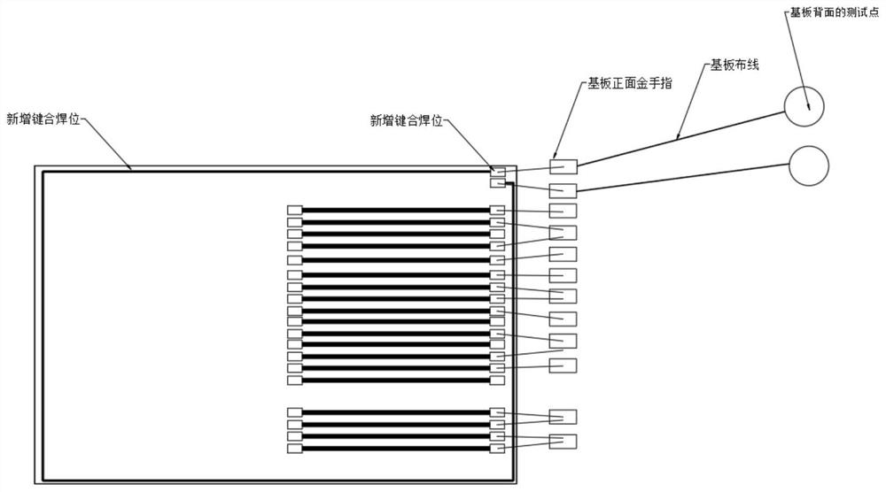
[0030] refer to Figure 1-4 , an LPDDR wafer RDL design method suitable for multi-chip failure analysis, including the following steps:

[0031] S1: Based on the conventional LPDDR RDL design, increase the bonding welding position;

[0032] Specifically, the conventional RDL is designed to guide the die edge from the middle pad to form a new pad.

[0033] S2: Design the packaging substrate and add several gold fingers on the front of the substrate for DIE connection;

[0034] S3: Encapsulate and connect the bonding pads with the gold fingers on the front of the substrate;

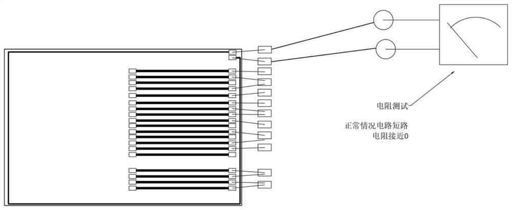
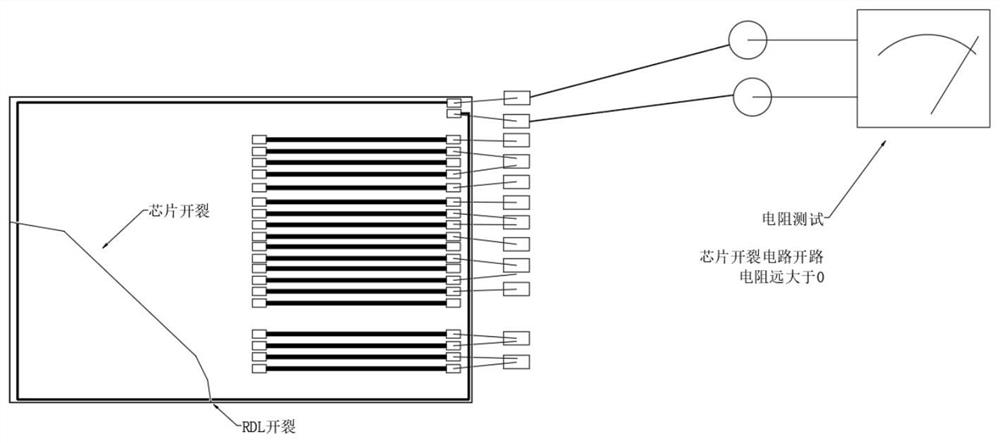
[0035] S4: Measure the resistance, judge the DIE state through ...


PUM


Abstract

The invention discloses an LPDDR wafer RDL design method suitable for multi-chip failure analysis, and belongs to the field of semiconductor packaging, and the method comprises the following steps: S1, based on a conventional LPDDR RDL design, adding a bonding welding position; s2, designing a packaging substrate, and adding a plurality of substrate front golden fingers for DIE connection; s3, packaging is carried out, the bonding welding positions are connected with the golden fingers on the front face of the substrate, S4, resistance is measured, the DIE state is judged through resistance testing, and design is completed. When the original RDL wiring is designed, the following RDL wiring is synchronously added; an unclosed square-shaped wire and two bonding pads (proper positions need to be found for the windowing positions of the bonding pads, and RDL wiring of an original product is not affected) are additionally arranged around the periphery of the DIE, whether the DIE cracks or not is judged through measurement data of wire resistance, a special testing machine is not needed, and the cost is reduced. The cracking of a certain DIE in the multi-chip stack can be judged only by using a universal meter or a simple test device to test the resistor.

Description

technical field [0001] The invention relates to the technical field of semiconductor packaging, in particular to an LPDDR wafer RDL design method suitable for multi-chip failure analysis. Background technique [0002] LPDDR is widely used in mobile consumer electronic products such as mobile phones and tablets, and the internal chip particles are packaged in a multi-layer stacking mode. In the actual production process, when the LPDDR wafer is stacked in a multi-layer package, an RDL will be done before wiring, and then packaging processes such as grinding, cutting, and chip stacking will be performed. The process of multi-layer stacking is relatively difficult, and it is prone to the problem of failure caused by single DIE cracking. [0003] In the existing technical solution, there are often multiple (2 to 8) DIEs with a thickness of only 200um to 40um stacked vertically inside an LPDDR package chip. Once a certain DIE cracks and fails, conventional testing machines canno...

Claims


Application Information

Patent Timeline
Patent Type & Authority Applications(China)
IPC IPC(8): H01L21/66H01L23/544
CPCH01L22/14H01L22/34H01L22/32
Inventor 张力廖承宇何洪文
Owner PAYTON TECHNOLOGY (SHENZHEN) CO LTD
Why Eureka
Try Eureka