Supercharge Your Innovation With Domain-Expert AI Agents!

Packaging structure with low dielectric constant solder mask layer and forming method thereof

A low dielectric constant, packaging structure technology, applied in the direction of circuits, electrical components, electrical solid devices, etc., can solve the problem that the dielectric constant of the solder mask cannot be reduced, and achieve the effect of reducing the dielectric constant and loss factor

Pending Publication Date: 2022-07-26
UNIMICRON TECH CORP
View PDF0 Cites 0 Cited by
  • Summary
  • Abstract
  • Description
  • Claims
  • Application Information

AI Technical Summary

Problems solved by technology

However, due to limited process requirements, the dielectric constant of the solder mask layer cannot be reduced

Method used


Image

  • Packaging structure with low dielectric constant solder mask layer and forming method thereof
  • Packaging structure with low dielectric constant solder mask layer and forming method thereof
  • Packaging structure with low dielectric constant solder mask layer and forming method thereof

Examples


Embodiment Construction

[0043] When an element is referred to as being "on", it can generally mean that the element is directly on the other element or that the other element is present in both. Conversely, when an element is referred to as being "directly on" another element, it cannot have the other element intervening. As used herein, the term "and / or" includes any combination of one or more of the associated listed items.

[0044] It will be understood that the terms first, second, and third, etc., are used herein to describe various elements, components, regions, layers and / or blocks. However, these elements, components, regions, layers and / or blocks should not be limited by these terms. These terms are only used to identify a single element, component, region, layer and / or block. Thus, a first element, component, region, layer and / or block hereinafter could be termed a second element, component, region, layer and / or block without departing from the intent of the present disclosure.

[0045] ...


PUM

PropertyMeasurementUnit
Diameteraaaaaaaaaa

Abstract

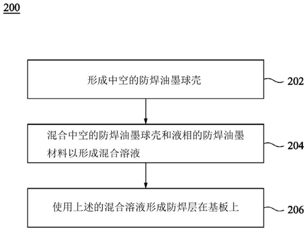
The invention relates to a packaging structure with a low dielectric constant solder mask layer and a forming method thereof. The packaging structure with the low-dielectric-constant solder mask layer comprises a substrate, a conductive structure located on the substrate and the solder mask layer located on the substrate. The solder mask layer comprises a plurality of bubbles and a solder mask ink material, the bubbles are fixed in the solder mask layer, and the solder mask ink material wraps the bubbles. Due to the fact that the bubbles have small dielectric properties, the bubbles are formed in the solder mask layer so as to effectively reduce the dielectric constant of the solder mask layer.

Description

technical field [0001] The present disclosure relates to a solder mask, especially a solder mask with a low dielectric constant in a package structure. Background technique [0002] In order to respond to the development trend of printed circuit boards, circuit board materials suitable for high frequency and high speed have become the primary goal of pursuing technological advancement in the future. Circuit board material parameters, such as copper layer thickness, copper surface roughness, substrate thickness, substrate dielectric constant, etc., are important factors that affect the process of high-frequency and high-speed signal transmission. Therefore, the industry has relevant countermeasures and development for the above factors. However, due to process requirements, the dielectric constant of the solder mask cannot be reduced. SUMMARY OF THE INVENTION [0003] According to some embodiments of the present disclosure, a package structure with a low-k solder mask incl...

Claims


Application Information

Patent Timeline
IPC IPC(8): H01L23/498H01L21/48
CPCH01L23/49811H01L23/49894H01L21/4846H01L21/4867
Inventor 吴明豪李国维
Owner UNIMICRON TECH CORP
Features
  • R&D
  • Intellectual Property
  • Life Sciences
  • Materials
  • Tech Scout
  • Unparalleled Data Quality
  • Higher Quality Content
  • 60% Fewer Hallucinations
Learn More