Reverse conducting IGBT (Insulated Gate Bipolar Translator) capable of eliminating voltage turn-back phenomenon

A reverse conduction type and phenomenon technology, applied in the field of power semiconductors, can solve the problems of uneven reverse conduction current distribution, low on-resistance, short length, etc., to eliminate snapback phenomenon, reverse conduction current uniformity, collector structure improved effect

Pending Publication Date: 2022-07-26
成都智达和创信息科技有限公司
View PDF0 Cites 0 Cited by
  • Summary
  • Abstract
  • Description
  • Claims
  • Application Information

AI Technical Summary

Problems solved by technology

[0002] like Figure 3-4 The conventional reverse conduction IGBT structure and equivalent circuit schematic diagram shown, when the traditional reverse conduction IGBT conducts forward, the N+ collector region (12) conducts first, and the device works in the unipolar conduction mode at this time, the conduction The resistance is relatively large. Due to the parasitic resistance of the N-type buffer layer (13), as the anode voltage increases, the anode current will generate a voltage drop on the parasitic resistance. When the potential difference between this voltage drop and the P+ collector region (11) is greater than 0.7 At V, the PN junction of the P+ collector region (13) / N-type buffer layer (13) is turned on, and the device enters a bipolar conduction mode with low on-resistance, and a sharp drop in on-resistance will cause voltage foldback , in order to alleviate this phenomenon, the length of the P+ collector region (11) of the conventional reverse conduction type IGBT is often designed to be very long, but this will cause the length of the N+ collector region (12) to be relatively short, and the reverse conduction type IGBT device reverse conductivity When on, the P+ body contact region (33), P-type well region (31), N-type drift region (21), N-type buffer layer (13) and N+ collector region (12) form a diode conduction current, at this time If the length of the N+ collector region (12) is short, it will lead to uneven distribution of reverse conduction current, which will affect device performance and system reliability

Method used


Image

  • Reverse conducting IGBT (Insulated Gate Bipolar Translator) capable of eliminating voltage turn-back phenomenon
  • Reverse conducting IGBT (Insulated Gate Bipolar Translator) capable of eliminating voltage turn-back phenomenon
  • Reverse conducting IGBT (Insulated Gate Bipolar Translator) capable of eliminating voltage turn-back phenomenon

Examples


Embodiment 1

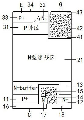
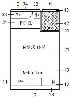
[0029] like Figure 1-2 A reverse-conducting IGBT that eliminates the phenomenon of voltage foldback as shown includes a half-cell structure, and the half-cell structure includes a collector structure, a voltage-resistant layer structure, an emitter structure, and a gate structure; the collector structure is located in the voltage-resistant layer structure. At one end, the emitter structure and the gate structure are located on both sides of the other end of the pressure-resistant layer structure, and the above content is not repeated here as the prior art;

[0030] The collector structure includes a P+ collector region 11, an N+ collector region 12, an N-type buffer layer 13, a P-type conductive material 15, a collector metal 16, an N-type conductive material 17 and a floating metal 18;

[0031] One side of the N-type buffer layer 13 is connected to the withstand voltage layer structure, one side of the P+ collector region 11 and the N+ collector region 12 are respectively co...

Embodiment 2

[0043] On the basis of Embodiment 1, further, a first insulating medium layer 14 is provided in the gap between the P+ collector region 11 and the N+ collector region 12 , and the P-type conductive material 15 is connected to the first insulating medium layer 14 superior.

[0044]Preferably, one side of the first insulating dielectric layer 14 is extended and attached to the N-type buffer layer 13 .


PUM


Abstract

The invention discloses a reverse conducting IGBT (Insulated Gate Bipolar Translator) capable of eliminating a voltage turn-back phenomenon, which comprises a semi-cellular structure, and the semi-cellular structure comprises a collector electrode structure, a voltage-withstanding layer structure, an emitter electrode structure and a grid electrode structure, the collector structure is located at one end of the voltage-withstanding layer structure, and the emitter structure and the gate structure are located at two sides of the other end of the voltage-withstanding layer structure; wherein the collector structure comprises a P + collector region, an N + collector region, an N-type buffer layer, a P + conductive material, collector metal, an N-type conductive material and floating metal; one side of the N-type buffer layer is connected to the voltage withstanding layer structure, one side of the P + collector region and one side of the N + collector region are connected to the other side of the N-type buffer layer, a gap is formed between the P + collector region and the N + collector region, and collector metal is arranged on the other side of the P + collector region; on the basis of a conventional reverse conducting IGBT structure, the snapback phenomenon is eliminated by optimizing and improving the collector electrode structure, and the reverse conducting current is more uniform.

Description

technical field [0001] The present invention relates to the field of power semiconductor technology, and more particularly to a reverse conduction IGBT which eliminates the phenomenon of voltage foldback. Background technique [0002] like Figure 3-4 The schematic diagram of the structure and equivalent circuit of the conventional reverse conduction IGBT shown, when the conventional reverse conduction IGBT is conducting forward, the N+ collector region (12) is turned on first. At this time, the device works in the unipolar conduction mode and is turned on. The resistance is relatively large. Due to the parasitic resistance of the N-type buffer layer (13), with the increase of the anode voltage, the anode current will produce a voltage drop on the parasitic resistance. When the potential difference between this voltage drop and the P+ collector region (11) is greater than 0.7 When V, the PN junction of the P+ collector region (13) / N-type buffer layer (13) is turned on, the...

Claims


Application Information

Patent Timeline
Patent Type & Authority Applications(China)
IPC IPC(8): H01L29/417H01L29/08H01L29/739H01L27/07
CPCH01L29/7398H01L29/7397H01L29/41708H01L27/0727H01L29/0821
Inventor 刘超余丽波孙瑞泽
Owner 成都智达和创信息科技有限公司
Why Eureka
Try Eureka