Double-pass wide-stop-band filter based on defected ground structure
A defect structure and filter technology, which is applied in the field of filters, can solve the problems of large influence of parasitic passbands and large size of filters, and achieve the effects of improving filtering performance, increasing stopband width, and reducing costs
- Summary
- Abstract
- Description
- Claims
- Application Information
AI Technical Summary
Problems solved by technology
Method used
Image
Examples
Embodiment
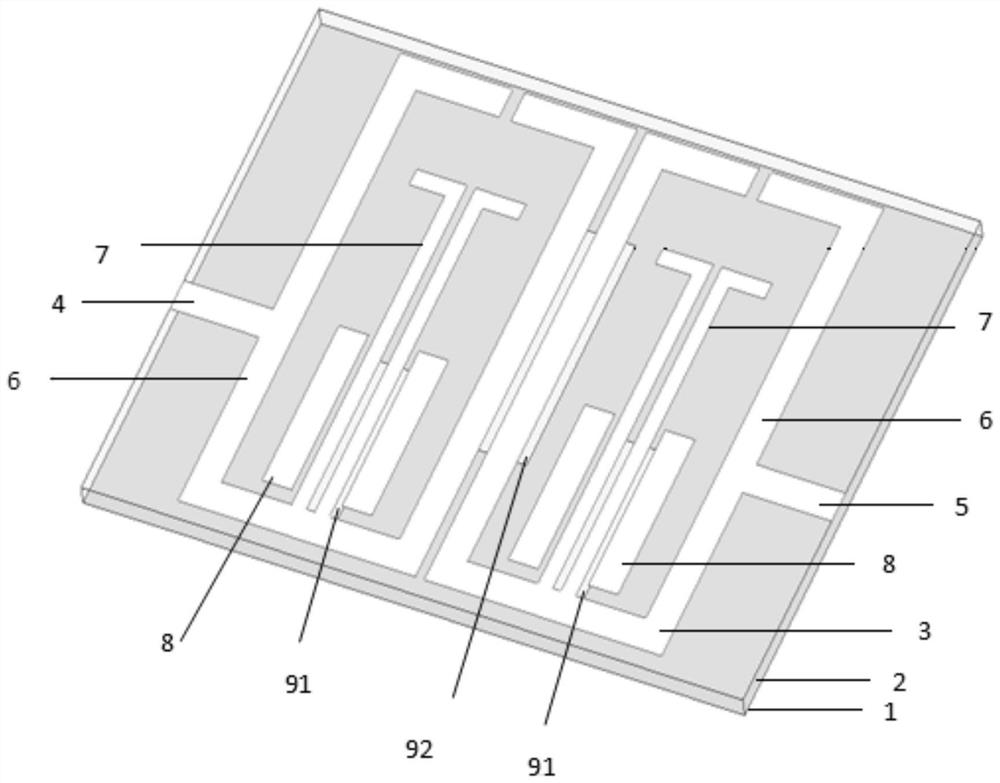
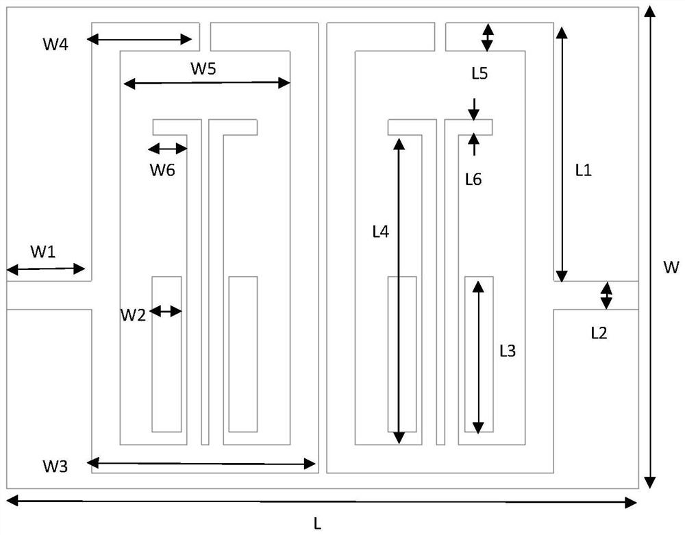
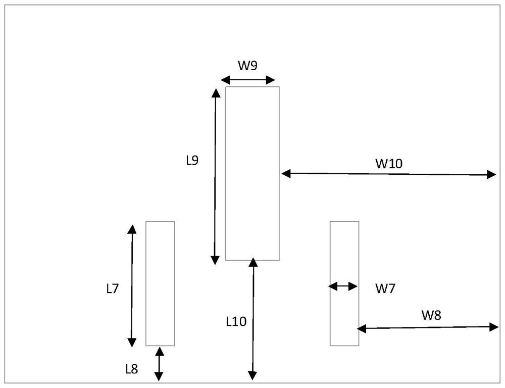
[0047] This embodiment takes the structure of a 3.3GHz-3.5GHz and 5.8GHz-6.1GHz double-pass filter as an example, wherein the dielectric constant of the dielectric layer 2 is 4.4 and the thickness is 1.6mm. like figure 2 and image 3 As shown, the size parameters of each structure on the filter layer 3 in the filter are as follows: W=17mm, W1=3mm, W2=1mm, W3=8mm, W4=3.8mm, W5=6mm, W6=1.2mm, W7 =1.28mm, W8=6.36mm, W9=2.4mm, W10=9.95mm, L=22.3mm, L1=9.1mm, L2=1mm, L3=5.5mm, L4=mm, L5=1mm, L6=0.55mm , L7=5.6mm, L8=1.65mm, L9=7.8mm, L10=5.5mm. The size of the low-pass filter is 22.3mm×17mm, and the filter has better miniaturization advantages.
[0048] Figure 4 The parameter simulation diagram of S11 and S12 obtained after the filter of the above structure and size is simulated and modeled in the electromagnetic software. It can be seen from the figure that the passband frequency of the filter is 3.23GHz-3.51GHz and 5.79GHz-6.28 GHz, in the passband, the in-band insertion l...
PUM
 Abstract
Description
Claims
Application Information


