Time sequence optimization circuit and method, chip and electronic equipment

An optimization method and timing technology, applied in electrical digital data processing, computer-aided design, instruments, etc., can solve problems such as timing problems not being optimized by tools, unsatisfactory timing optimization effects, and chip performance affecting project progress, etc., to achieve Improve timing optimization effects, shorten design time, and solve timing problems

Pending Publication Date: 2022-08-02
GUANGDONG OPPO MOBILE TELECOMM CORP LTD
View PDF0 Cites 4 Cited by
  • Summary
  • Abstract
  • Description
  • Claims
  • Application Information

AI Technical Summary

Problems solved by technology

With the support of powerful Electronics Design Automation (EDA) tools, most of the timing problems can be solved automatically. However, when chip design enters the Engineering Change Order (ECO) stage, it is inevitable that some The timing problem is not optimized by the tool
[0003] At present, for the remaining timing violations in the ECO stage, common optimization methods such as optimizing the data path, extending or shortening the clock tree, etc., the effect of timing optimization is not ideal, which seriously affects the progress of the project and chip performance.

Method used


Image

  • Time sequence optimization circuit and method, chip and electronic equipment
  • Time sequence optimization circuit and method, chip and electronic equipment
  • Time sequence optimization circuit and method, chip and electronic equipment

Examples


Embodiment Construction

[0030] The technical solutions in the embodiments of the present application will be clearly and completely described below with reference to the accompanying drawings in the embodiments of the present application. It should be understood that the specific embodiments described herein are only used to explain the related application, but not to limit the application. In addition, it should be noted that, for the convenience of description, only the parts related to the relevant application are shown in the drawings.

[0031] Before further describing the embodiments of the present invention in detail, the terms and terms involved in the embodiments of the present invention are described. The terms and terms involved in the embodiments of the present invention are applicable to the following explanations.

[0032] Place and route (Place and Route, PnR). Among them, Place is the layout, and Route is the wiring.

[0033] Electronic Design Automation (EDA) refers to the use of C...


PUM


Abstract

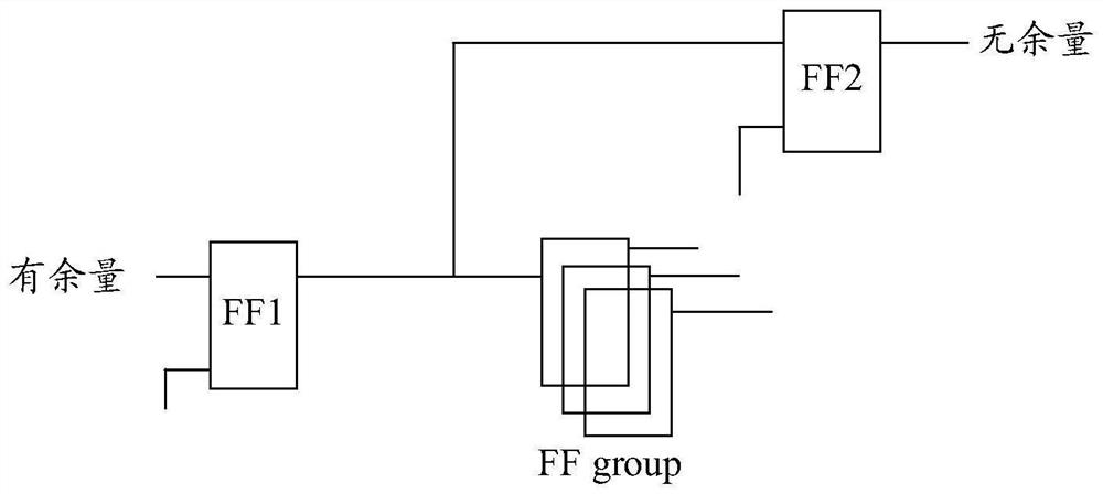
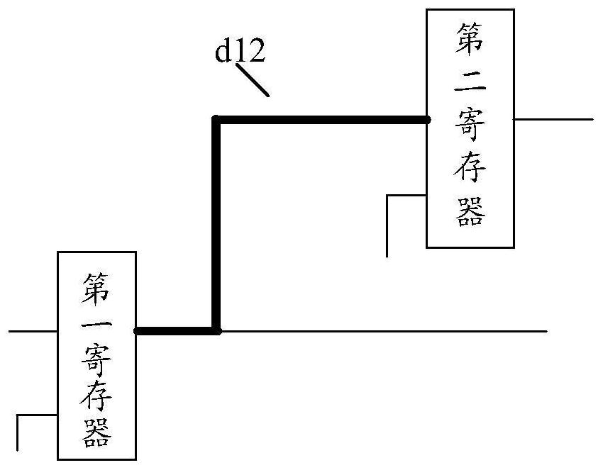
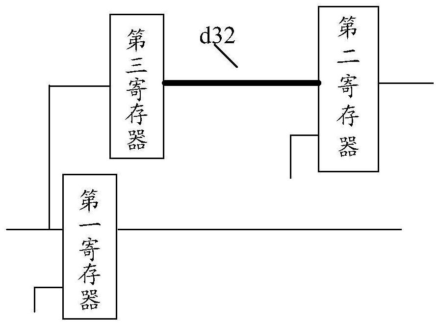
The embodiment of the invention discloses a time sequence optimization circuit and method, a chip and electronic equipment, the electronic equipment comprises the chip provided with the time sequence optimization circuit, the time sequence optimization circuit comprises a first register, a second register and a third register, and the third register is a duplicated register of the first register; the path distance between the first register and the second register is greater than that between the third register and the second register; when a time sequence report obtained by executing the time sequence analysis command indicates that time sequence violation exists in the first time sequence path, the second time sequence path is used for performing time sequence optimization processing; the path starting point of the first time sequence path is a first register, and the path end point is a second register; the path starting point of the second time sequence path is the third register, and the path end point is the second register. The time sequence optimization method comprises the following steps: executing a time sequence analysis command to obtain a time sequence report; and when the time sequence report indicates that the time sequence violation exists in the first time sequence path, performing time sequence optimization processing through the second time sequence path.

Description

technical field [0001] The present invention relates to the technical field of integrated circuit design, in particular to a timing optimization circuit and method, a chip and an electronic device. Background technique [0002] As the scale of chip design becomes larger, the competition becomes more intense, the timing closure becomes more and more complicated, and the requirements for the back-end design of the chip become higher and higher. With the support of powerful Electronic Design Automation (EDA) tools, most of the timing problems can be solved automatically. However, when the chip design enters the Engineering Changing Order (ECO) stage, it is inevitable that some individuals will be left behind. The timing problem is not optimized by the tool. [0003] At present, for the remaining timing violations in the ECO stage, common optimization methods such as optimizing the data path, extending or shortening the clock tree, etc., the effect of timing optimization is not...

Claims


Application Information

Patent Timeline
Patent Type & Authority Applications(China)
IPC IPC(8): G06F30/3315G06F30/337G06F30/392G06F30/394
CPCG06F30/3315G06F30/337G06F30/392G06F30/394
Inventor 南鹏飞
Owner GUANGDONG OPPO MOBILE TELECOMM CORP LTD
Why Eureka
Try Eureka