Digital-analog converter, circuit board, electronic device, and liquid crystal display unit
A digital-to-analog converter, digital signal conversion technology, applied in the direction of digital-to-analog converter, analog-to-digital conversion, electrical components, etc., can solve problems such as high power consumption, and achieve the effect of reducing power consumption
- Summary
- Abstract
- Description
- Claims
- Application Information
AI Technical Summary
Problems solved by technology
Method used
Image
Examples
Embodiment 1
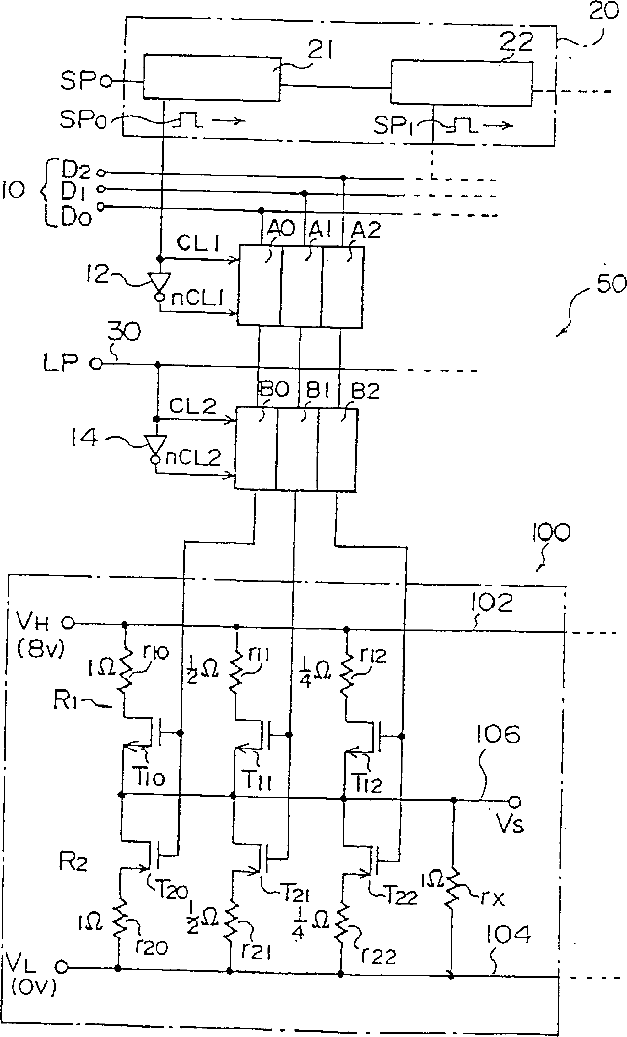
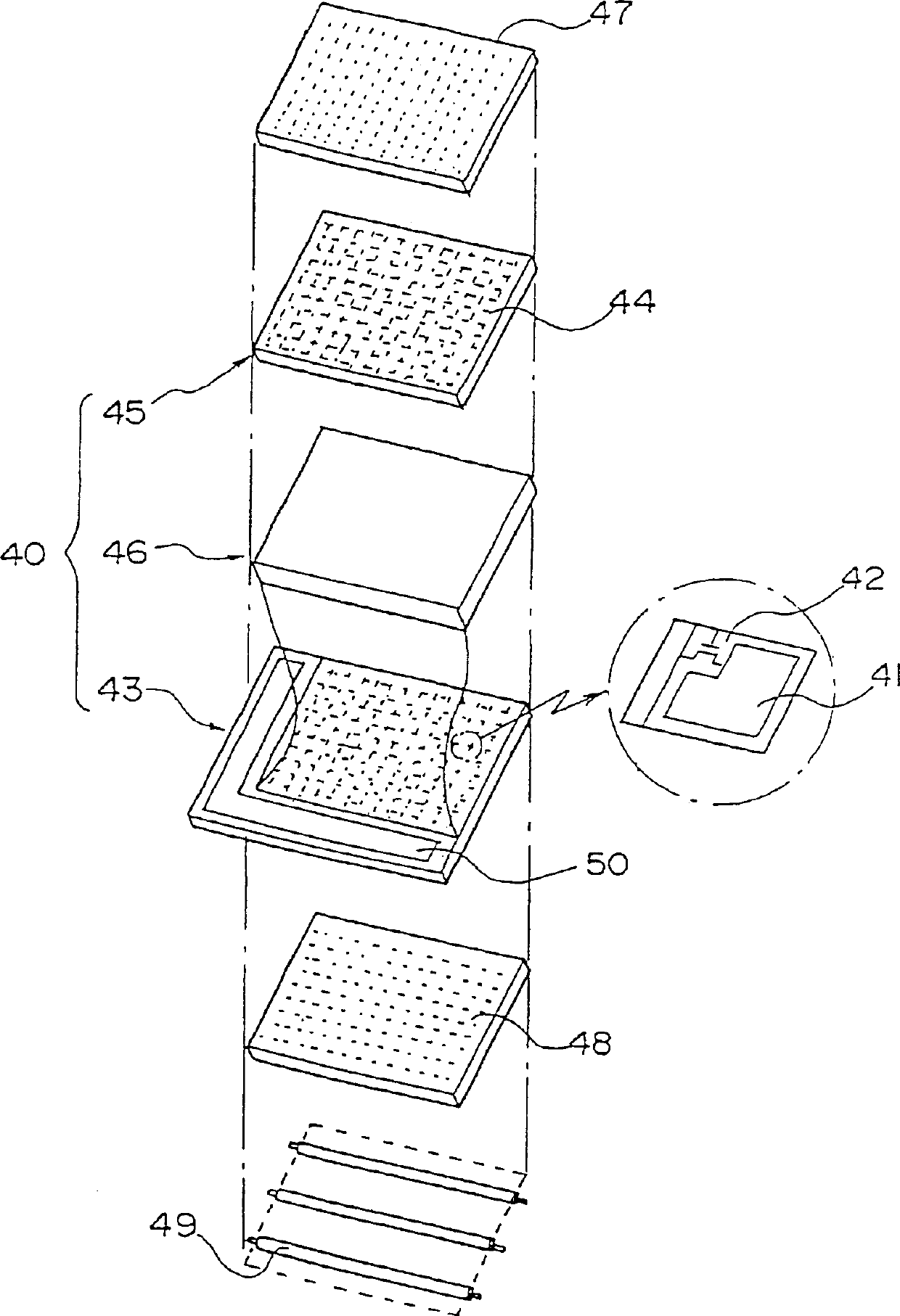
[0095] FIG. 1 shows a driving circuit of a liquid crystal display device according to a first embodiment. In addition, FIG. 2 shows an exploded perspective view of the liquid crystal display device. As shown in FIG. 2, this liquid crystal display device has a liquid crystal panel 40 of an active matrix type. The liquid crystal panel 40 is formed by sealing a liquid crystal 46 between a TFT substrate 43 having a thin film transistor 42 each controlling a power supply of a potential of a pixel electrode and a color filter substrate 45 having a counter electrode 44. In addition, deflection plates 47 and 48 are installed on both surfaces of the liquid crystal panel 40 , and a backlight 49 is installed on one side of the deflection plate 48 . Furthermore, a driver circuit 50 is formed on the TFT substrate 43 .
[0096] As shown in FIG. 1 , the driving circuit 50 includes a digital-to-analog conversion circuit 100 according to the present invention. The digital-to-analog conversi...
Embodiment 2
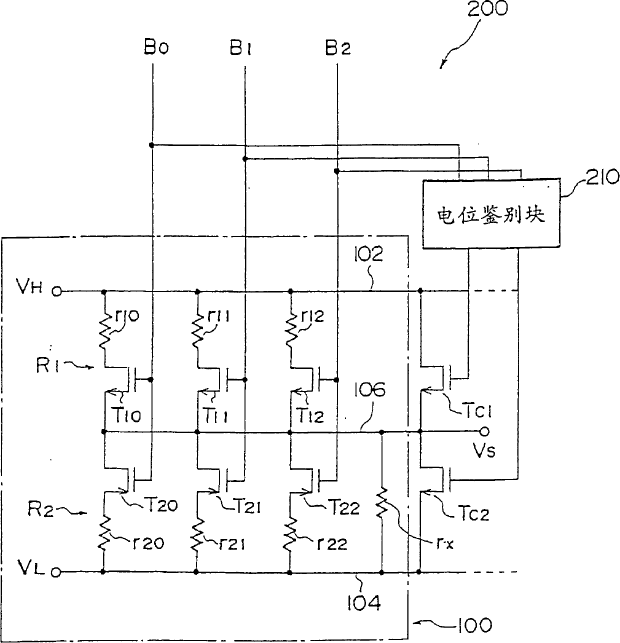
[0150] FIG. 5 is a circuit diagram showing a digital-to-analog conversion circuit according to a second embodiment. The digital-to-analog conversion circuit 200 is formed by adding a potential discriminating block 210 and precharge switches TC1 and TC2 to the digital-to-analog conversion circuit 100 .
[0151] The pre-charge switch TC1 is between the high potential line 102 and the output line 106 , and the pre-charge switch TC2 is between the output line 106 and the low potential line 104 .
[0152] If the pre-charge switch TC1 is on and the pre-charge switch TC2 is off, the analog output signal V of the output line 106 Sbecomes the potential V of the high potential line 102 H same potential. Therefore, if the analog output signal V corresponding to the digital signal S close to the potential V H , then in this way the analog output signal V S set to the potential V H . Then, it is possible to obtain an appropriate analog output signal V by using variable resistor bloc...
Embodiment 3
[0165] FIG. 6 is a circuit diagram showing a digital-to-analog conversion circuit according to a third embodiment. The digital-to-analog conversion circuit 300 is formed by adding a potential adjustment block 310 to the digital-to-analog conversion circuit 100 .
[0166] The potential adjustment block 310 controls the respective potentials V of the high potential line 102 and the low potential line 104 H and V L The change. Therefore, the analog output signal V S range can be changed.
[0167] For example, in the first embodiment, the potential V H set to 8V, V L is set to 0V, therefore, the analog output signal V S Varies from 0 to 7V. If the potential V H becomes 16V, V L becomes 8V, therefore, the analog output signal V S becomes variable in the range of 8 to 15V. Then, without changing the structure of the variable resistance block R1 and R2, it is possible to obtain the analog output signal V in the range of 0 to 16V S .
PUM
 Abstract
Description
Claims
Application Information


