Printing head substrate, printing head, printing head box and its printer

A print head and substrate technology, applied in printing, automatic power control, electrical components, etc., can solve problems such as interference with high-speed data transmission

Inactive Publication Date: 2004-12-01
CANON KK
View PDF9 Cites 0 Cited by
  • Summary
  • Abstract
  • Description
  • Claims
  • Application Information

AI Technical Summary

Problems solved by technology

This becomes the cause of malfunction and interferes with high-speed data transmission

Method used


Image

  • Printing head substrate, printing head, printing head box and its printer
  • Printing head substrate, printing head, printing head box and its printer
  • Printing head substrate, printing head, printing head box and its printer

Examples


no. 1 example

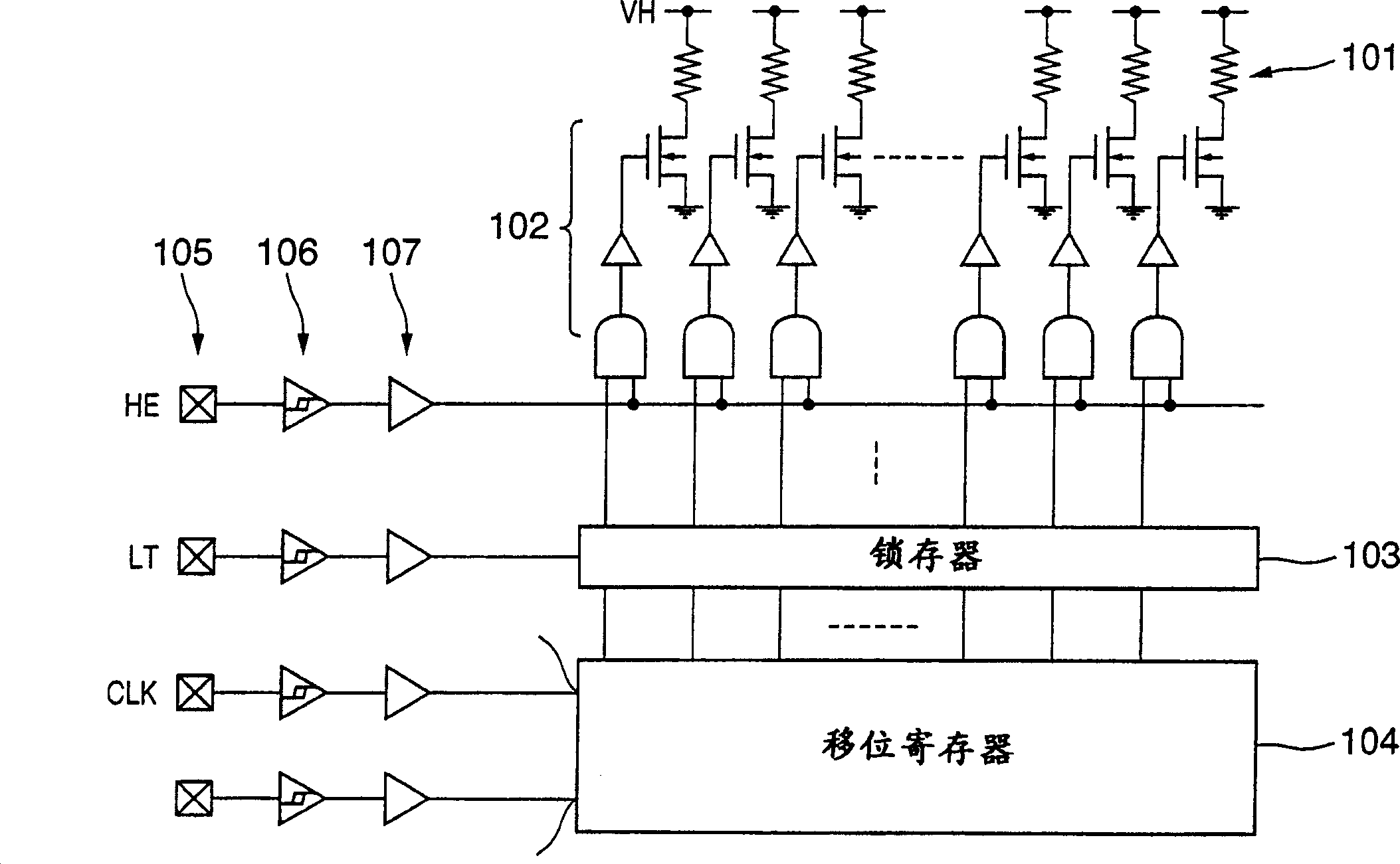
[0060] Figure 9 is a block diagram showing the construction of the print head chip according to the first embodiment of the present invention. for figure 2 Elements that are common to those shown in are denoted by the same reference numerals.

[0061] Each of the printhead dies 901 through 906 has afigure 1 The same circuit arrangement as the printhead die represented in . Assume that printing is performed by using six sheets of substrates 901 to 906 .

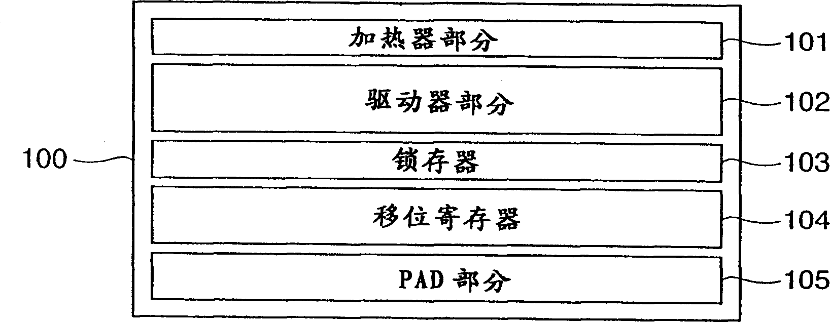
[0062] exist Figure 9 Among them, reference numeral 101 designates a heater portion (heater element) serving as an electrothermal transducer, reference numeral 102 designates a driver portion for driving each heater element according to print data, reference numeral 103 designates a latch circuit for latching print data, and reference numeral 103 designates a latch circuit for latching print data. 104 denotes a shift register that stores and holds a DATA signal serially input in synchronization with the CLK signal, and ...

no. 2 example

[0069] Figure 10 is a circuit diagram showing the wiring of the DATA signal and the CLK signal on the print head chip according to the second embodiment of the present invention. for Figure 9 Elements common to those shown in are denoted by the same reference numerals, and descriptions thereof are omitted.

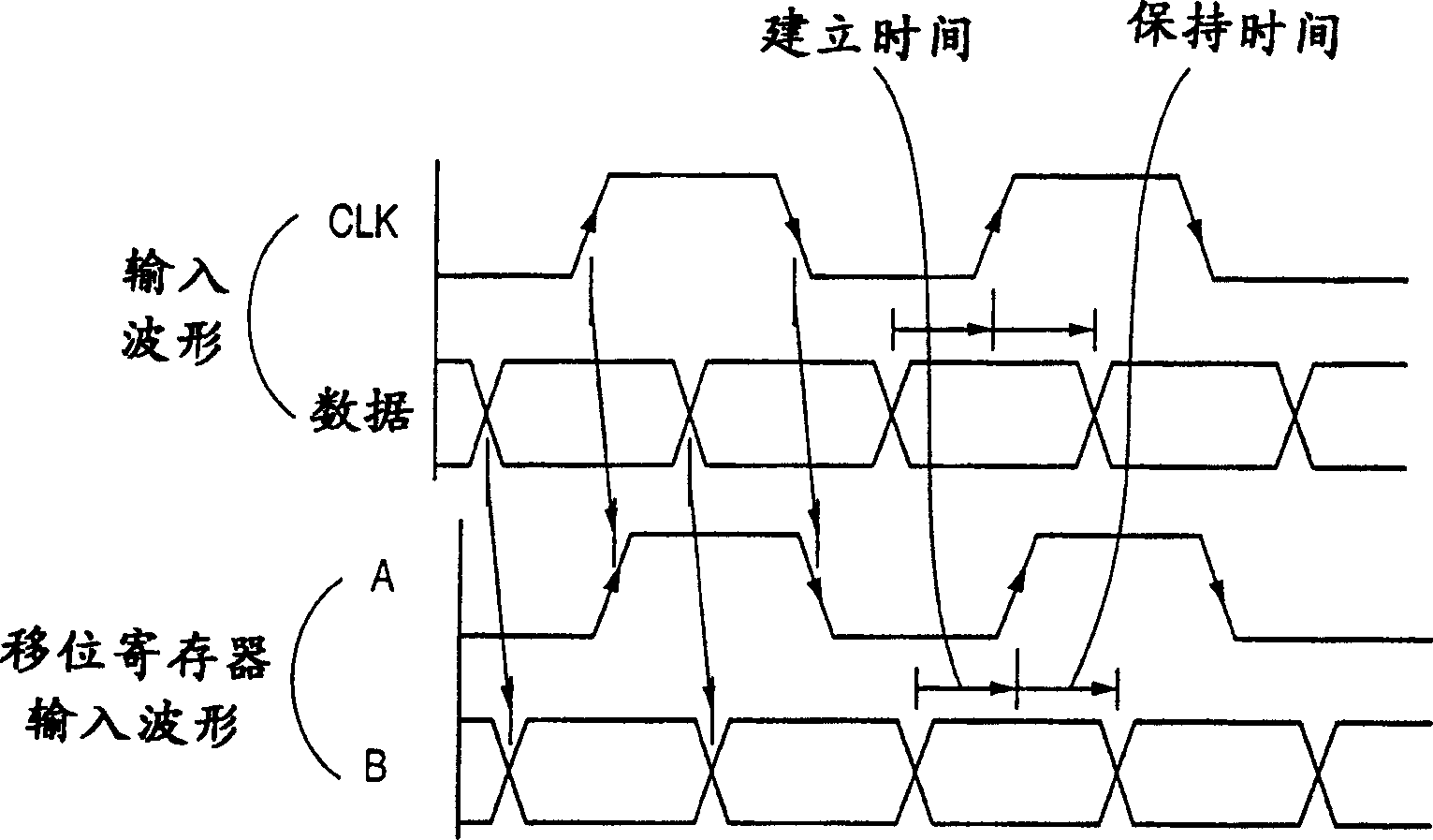
[0070] Figure 10 One capacitor 911 is shown connected to each output of buffer 107 for each DATA signal, as an example of time lag adjuster 910 . Here, it is assumed that the capacitance of each capacitor 911 is CL, and the input capacitances at the DATA input terminal and the CLK input terminal of each shift register 110 are CDATA and CCLK, respectively. It is further assumed that the on-resistances of the DATA signal and the CLK signal when driving the buffer circuit 107 are RDATA and RCLK, respectively, and that the number of shift registers 110 commonly connected to the CLK signal is n. Here, the time lag TDATA of the DATA signal input to each shift register 110...

no. 3 example

[0077] Figure 11 is a circuit diagram showing the wiring of the DATA signal and the CLK signal on the print head chip according to the third embodiment of the present invention. for Figure 9 and 10 Elements common to those shown in are denoted by the same reference numerals, and descriptions thereof are omitted.

[0078] Figure 11 One resistor 912 is shown connected to each output of buffer 107 for each DATA signal, as an example of time lag regulator 910 . Assuming that the resistance value of each resistor 912 is RL, the time lag TDATA of the DATA signal input to each shift register and the time lag TCLK of the CLK signal are described as follows:

[0079] TDATA≈(RDATA+RL)×CDATA

[0080] TCLK≈n×RCLK×CCLK

[0081] Here, the resistance value RL is set as follows:

[0082] RL=(n×RCLK×CCLK) / CDATA-RDATA

[0083] As a result, TDATA=TCLK holds true. With this, the difference between the time lag of the DATA signal input to each shift register 110 and the time lag of the...


PUM


Abstract

The invention relates to a printing head substrate, a printing head, a printing head box and its printer, wherein the printhead substrate for inputting a data signal (DATA) in synchronization with a clock signal (CLK). The printing head substrate comprises: input terminals inputting the clock signal and data signal; shift registers inputting and maintaining the data signal in synchronization with the clock signal inputted from the input terminals; and a time lag adjuster arranged between an input terminal and the shift register to adjust a time lag of at least one of the clock signal or data signal. By virtue of adjusting the time lag by the time lag adjuster, setup time and hold time between the clock signal and the data signal inputted to the shift register is ensured.

Description

technical field [0001] The present invention relates to a print head substrate for inputting a data signal synchronously with a clock signal, a print head, a print head cartridge, and a printer thereof. Background technique [0002] figure 1 and 2 A layout diagram and a circuit diagram of a conventional inkjet printing head for inputting a data signal in synchronization with a clock signal are respectively shown. [0003] refer to figure 1 , the print head substrate (heater board) 100 includes: a heater part 101, which is used as an electrothermal transducer; a driver part 102, with a transistor for driving the heater part 101; a latch 103, which latches For print data, a shift register 104 stores serially input print data; and a PAD section 105 serves as an input terminal into which various signals are input. [0004] figure 2 yes figure 1 The circuit diagram of the heater board 100 shown in . for figure 1 Elements common to those represented in are indicated with ...

Claims


Application Information

Patent Timeline
Patent Type & Authority Patents(China)
IPC IPC(8): B41J2/01B41J2/05B41J2/14
CPCB41J2/04541B41J2/0452B41J2/0458B41J2/14072B41J2/0457B41J2/04546B41J2/04548B41J2/04543B41J2/0455B41J2/04521B41J2/01
Inventor 平山信之古川達生今仲良行
Owner CANON KK
Why Eureka
Try Eureka