Single-crystal 2X2 photo switch
An optical switch and crystal technology, applied in optics, nonlinear optics, instruments, etc., can solve problems such as large loss of light
- Summary
- Abstract
- Description
- Claims
- Application Information
AI Technical Summary
Problems solved by technology
Method used
Image
Examples
example 1
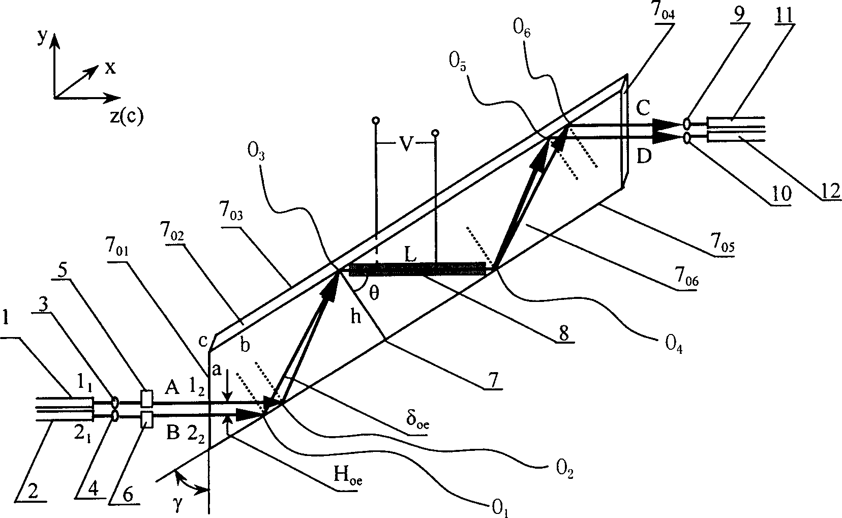
[0047] Example 1: If figure 1 structure shown. The size of crystal 7 is 9×4×0.2cm 3 , beam input facet 7 01 with the second reflective surface 7 05 The included angle γ=θ=40°, the central optical axis of the two incident lights is 1 1 1 2 and 2 1 2 2 The distance between Hoe=0.15cm, electrode length L=3.4cm, half-wave voltage V 1 / 2 = 235V (aspect ratio of 1:17).
example 2
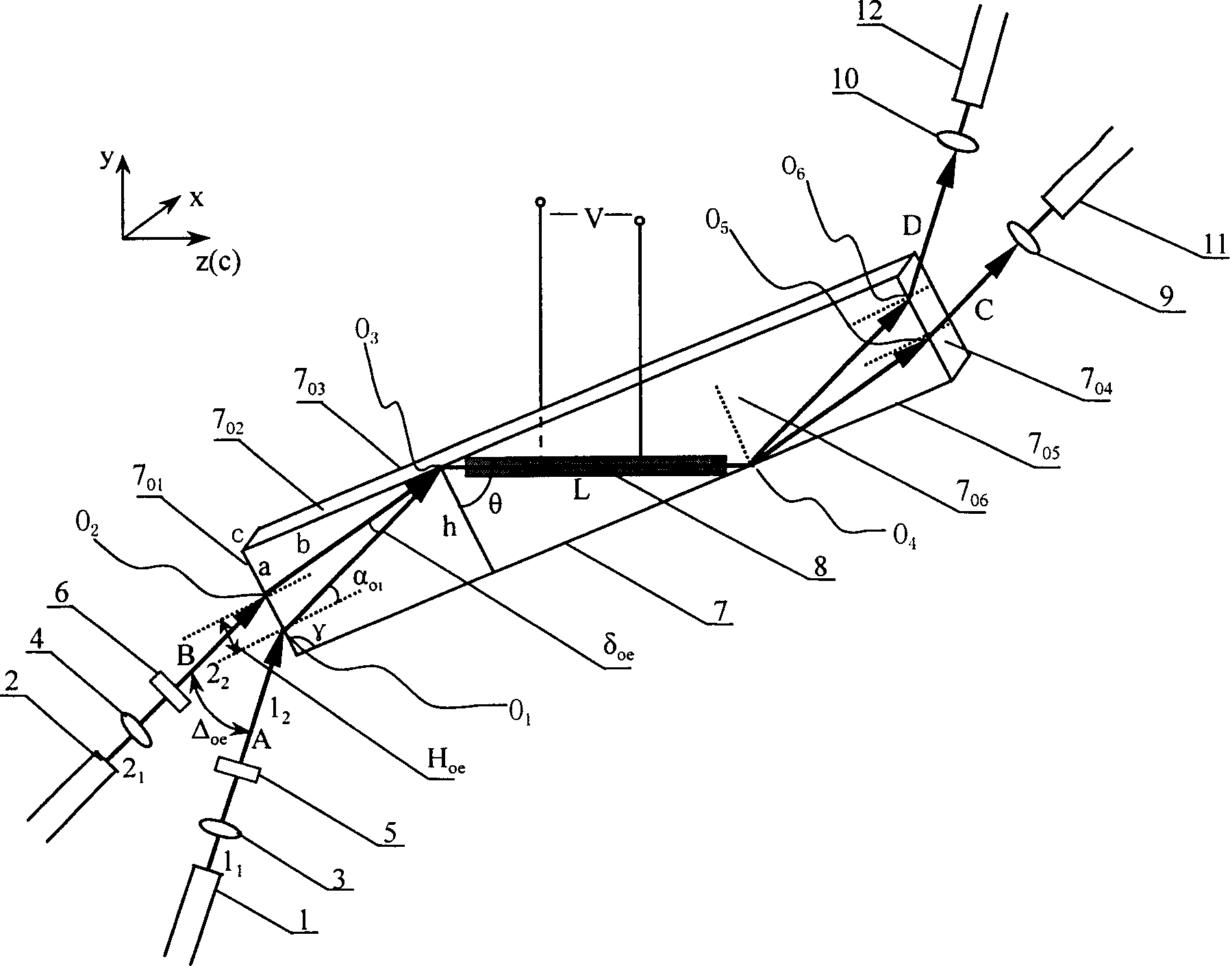
[0048] Example 2: If figure 2 structure shown. The crystal size is 7.4×1.5×0.2cm 3 , beam input facet 7 01 with the second reflective surface 7 05 The included angle γ=110°, θ=70°, the light path A is vertically incident (α ol =0°), two incident light central optical axis 1 1 1 2 and 2 1 2 2 The angle between them is Δoe=5.4°, the two incident lights are on the beam input surface 7 01 Hoe=0.01cm, electrode length L=4.1cm, half-wave voltage V 1 / 2 =195V (aspect ratio of 1:20.5).
PUM
 Abstract
Description
Claims
Application Information


