

Production method of film circuit plate
A thin-film circuit board and circuit technology, which is applied in the manufacture of printed circuits, printed circuits, electrical components, etc., can solve problems such as inconvenience for users, poor product reliability, and many printing processes.
- Summary
- Abstract
- Description
- Claims
- Application Information
AI Technical Summary
Problems solved by technology
Method used
Image

Examples
Embodiment Construction
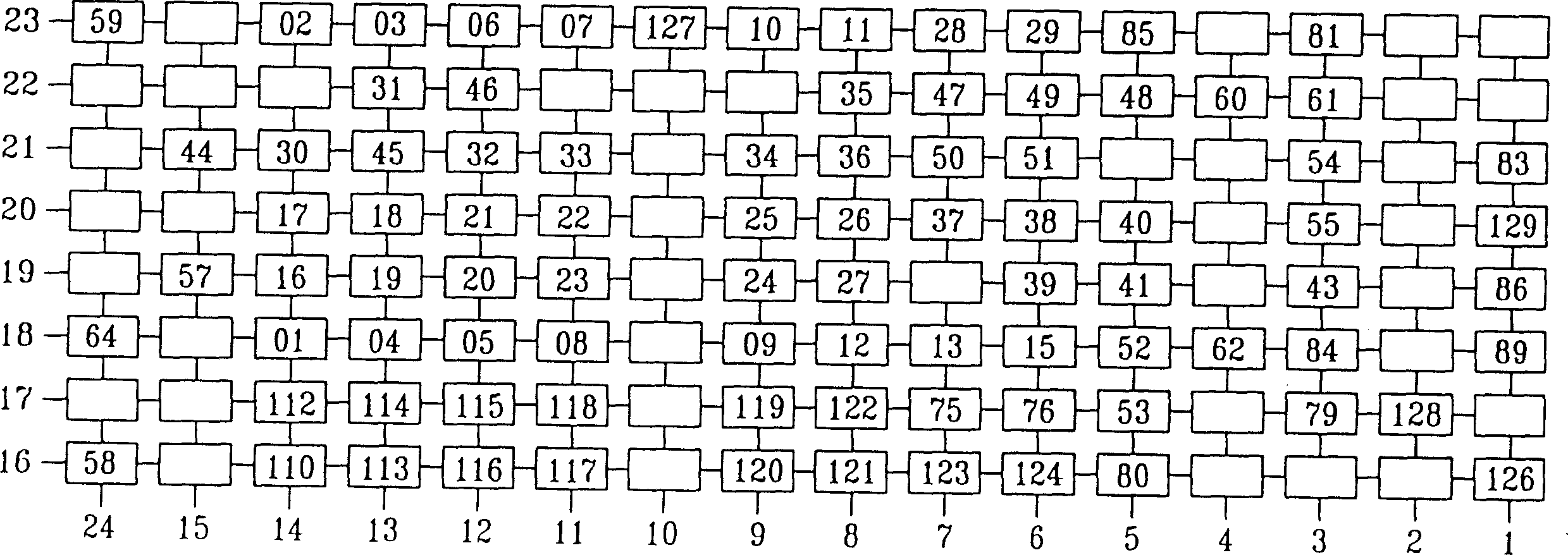
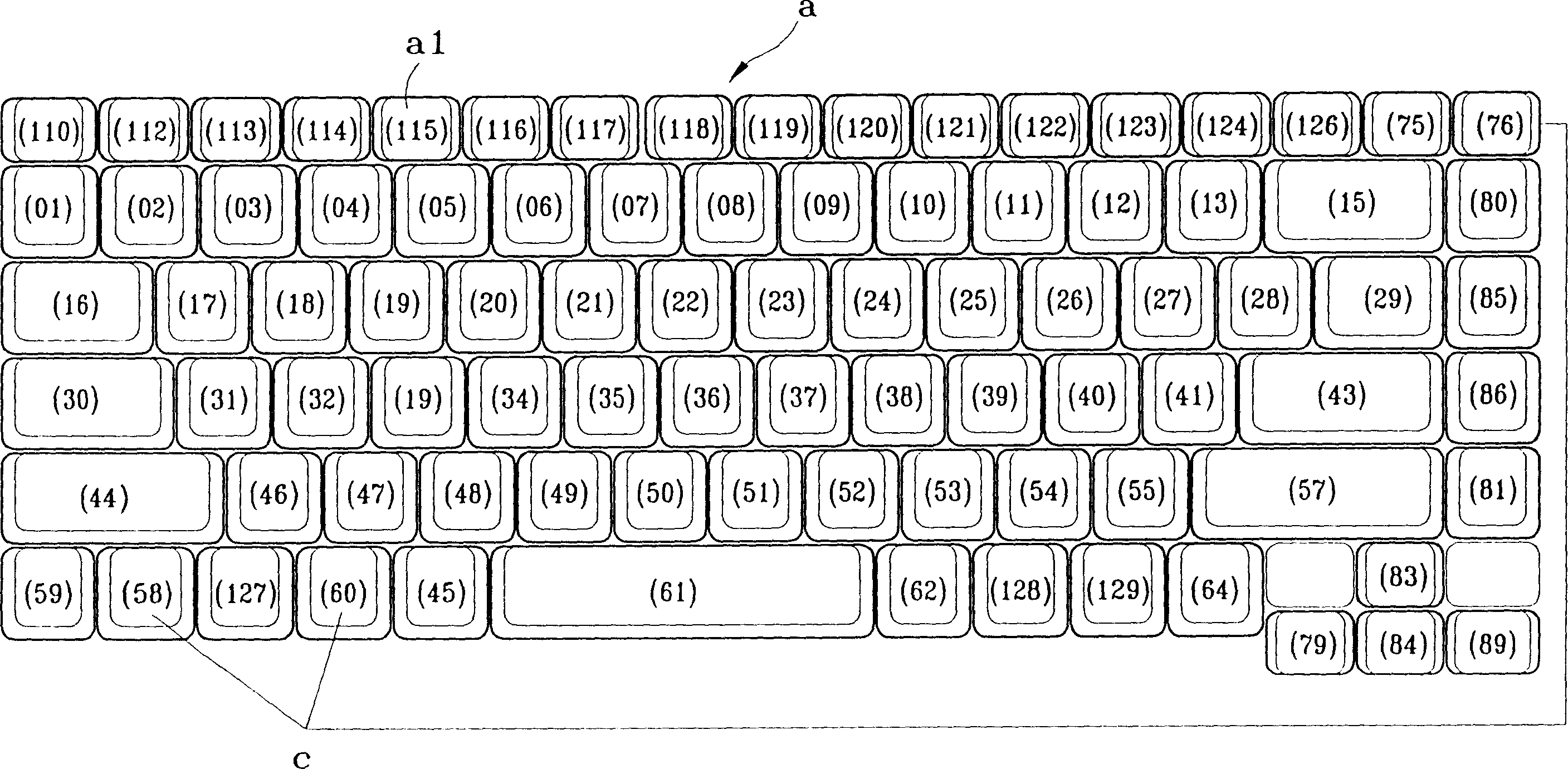
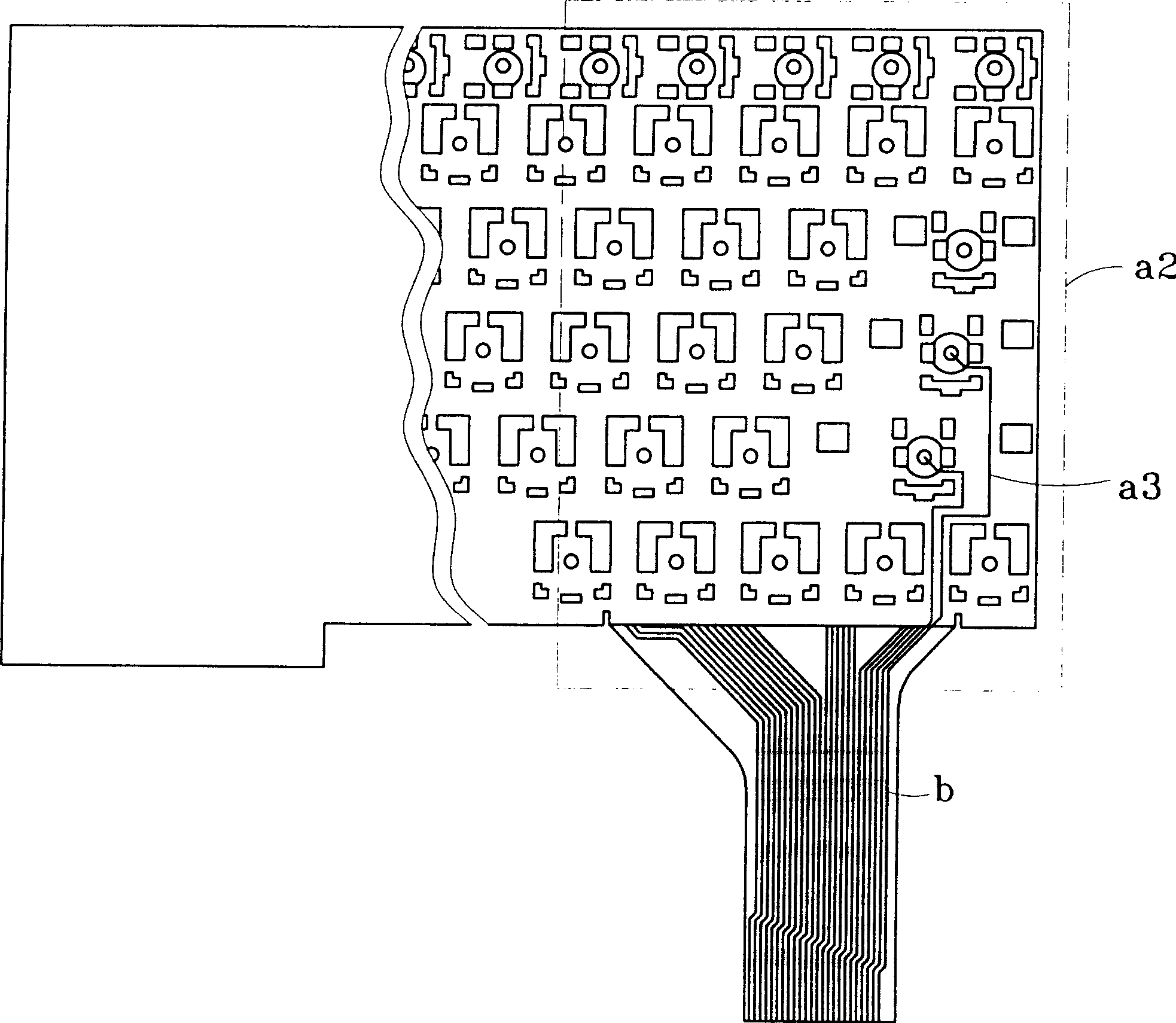
[0015] see figure 2 , 3 , is a schematic diagram of key position distribution and thin film circuit board of the present invention. As shown in the figure: the manufacturing method of the thin film circuit board of the present invention is mainly carried out under the condition that the thin film circuit board does not jump wires and avoids the generation of unknown key signals when the thin film circuit board is arranged or arranged (Membrane Layout) to make. Circuit arrangement (Layout), and then define the matrix (Matrix) arrangement, and then provide the manufacturer to fill in the code of each key position in the chip; this production method can reduce the circuit board printing process, reduce production costs, and increase production. Relatively, the production steps are also reduced, thereby reducing the loss caused by the defect rate, and at the same time, it can also avoid the micro-short circuit caused by the free circuit of the jumper part, which can improve the ...
PUM
 Abstract
Description
Claims
Application Information