Substrate processing device, liquid processing device and liquid processing method
A substrate processing and processing liquid technology, applied in optics, instruments, electrical components, etc., can solve problems such as difficult stop conditions, enlarged photocopying of developing devices, and large loads on LCD substrates
- Summary
- Abstract
- Description
- Claims
- Application Information
AI Technical Summary
Problems solved by technology
Method used
Image
Examples
Embodiment 1
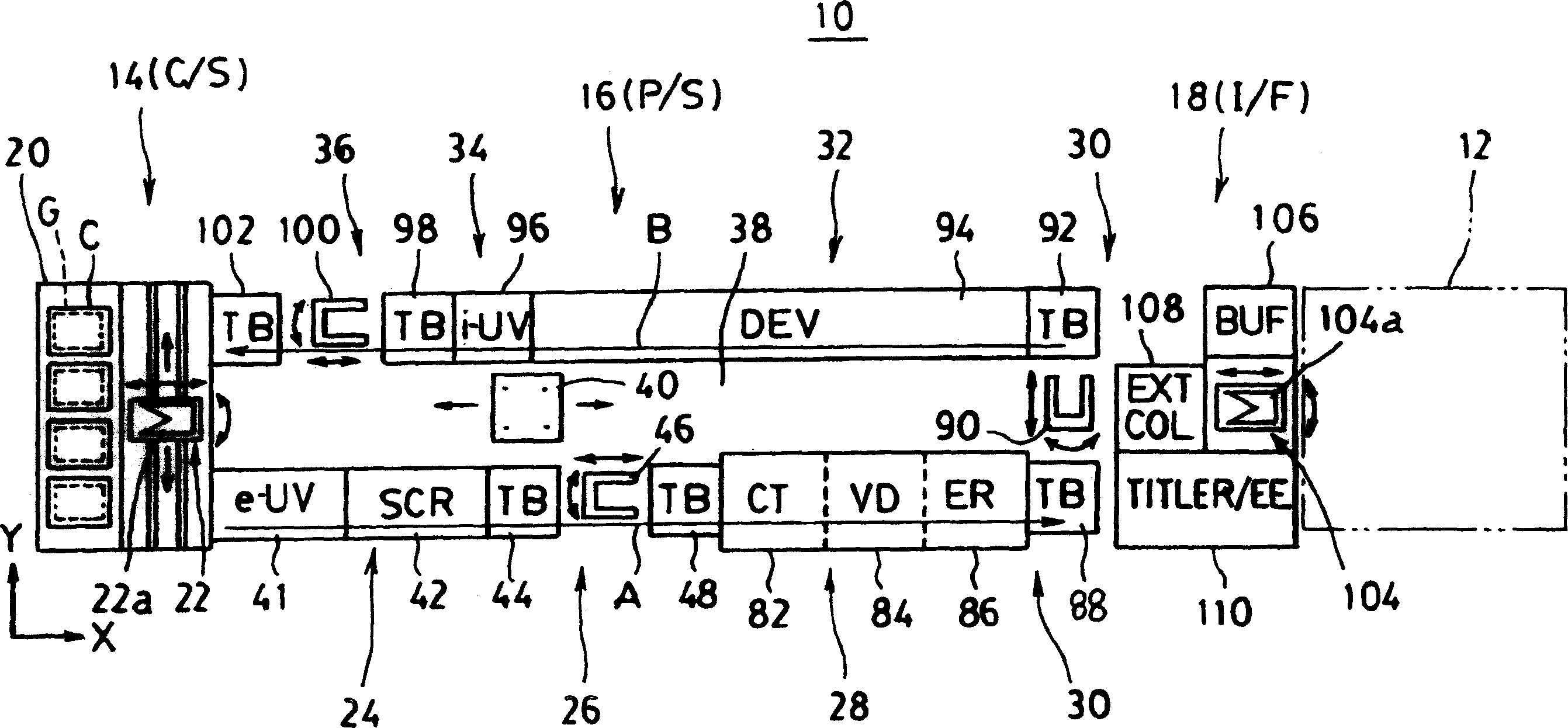
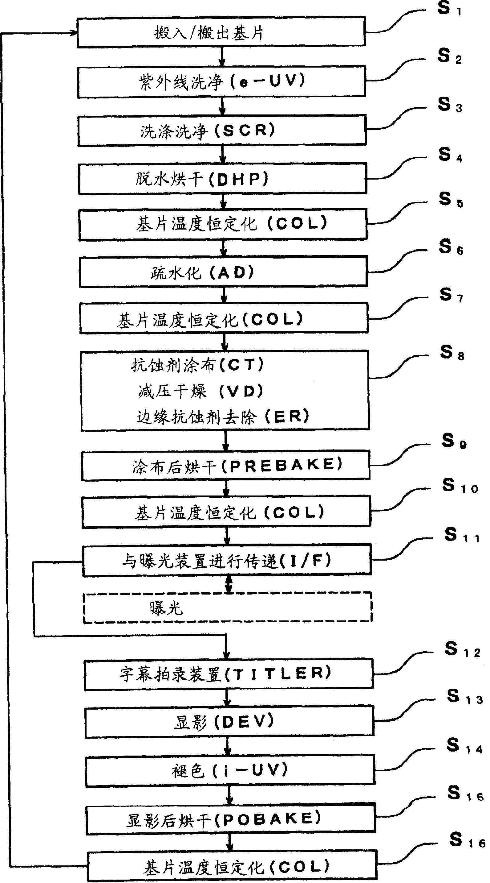
[0073] figure 1 A coating development processing system is shown as an example of the structure to which the developing processing apparatus of the present invention is applied. The coating and development processing system 10 is installed in a clean room, and for example, an LCD substrate is used as a substrate to be processed. In the LCD manufacturing process, cleaning, resist coating, pre-drying, and developing are performed in the lithography process. And post-drying and other treatments. Exposure processing is performed by an external exposure device 12 provided adjacent to the system.
[0074] In this coating and development processing system 10, a horizontally long processing station (P / S) 16 is arranged at the center, and a disc cartridge station (C / S) 14 and an interface station ( I / F) 18.
[0075] The disk cartridge station (C / S) 10 is the disk cartridge loading and unloading end of the system 10. It is equipped with multi-stage overlapping substrates G and loads ...
Embodiment 2
[0178] Embodiments of the present invention will be described in detail below with reference to the drawings. Here, in this embodiment, a case where the present invention is applied to a developing unit (DEV) for developing an exposed LCD substrate will be described as an example. Figure 19 It is a schematic plan view showing a resist coating and development processing system having a development processing unit (DEV) as an embodiment of the present invention, and continuously performing resist coating and development processing from resist film formation to development processing.
[0179] This resist coating and development processing system 400 has: a disk cartridge table (carry-in and carry-out part) 301 on which a disk cartridge C accommodating a plurality of LCD substrates G is loaded; a processing table (processing part) 302 has a plurality of processing units, A series of processes including resist coating and development are performed on the LCD substrate G; the inte...
PUM
 Abstract
Description
Claims
Application Information
 - R&D
- Intellectual Property
- Life Sciences
- Materials
- Tech Scout
- Unparalleled Data Quality
- Higher Quality Content
- 60% Fewer Hallucinations
Browse by: Latest US Patents, China's latest patents, Technical Efficacy Thesaurus, Application Domain, Technology Topic, Popular Technical Reports.
© 2025 PatSnap. All rights reserved.Legal|Privacy policy|Modern Slavery Act Transparency Statement|Sitemap|About US| Contact US: help@patsnap.com


