
Longitudinal transistor, memory device and longitudinal transistor making process

A technology of vertical transistors and channel regions, applied in semiconductor/solid-state device manufacturing, electrical solid-state devices, semiconductor devices, etc., can solve the problems of time-consuming manufacturing methods and troubles, and achieve reduced manufacturing costs, high packaging density, and reduced location. effect of demand

Inactive Publication Date: 2006-07-19
INFINEON TECH AG
View PDF0 Cites 3 Cited by
  • Summary
  • Abstract
  • Description
  • Claims
  • Application Information

AI Technical Summary

Problems solved by technology

Complicated and time-consuming production methods therefore arise for the known vertical transistors

Method used


Image

  • Longitudinal transistor, memory device and longitudinal transistor making process
  • Longitudinal transistor, memory device and longitudinal transistor making process
  • Longitudinal transistor, memory device and longitudinal transistor making process

Examples


Embodiment Construction

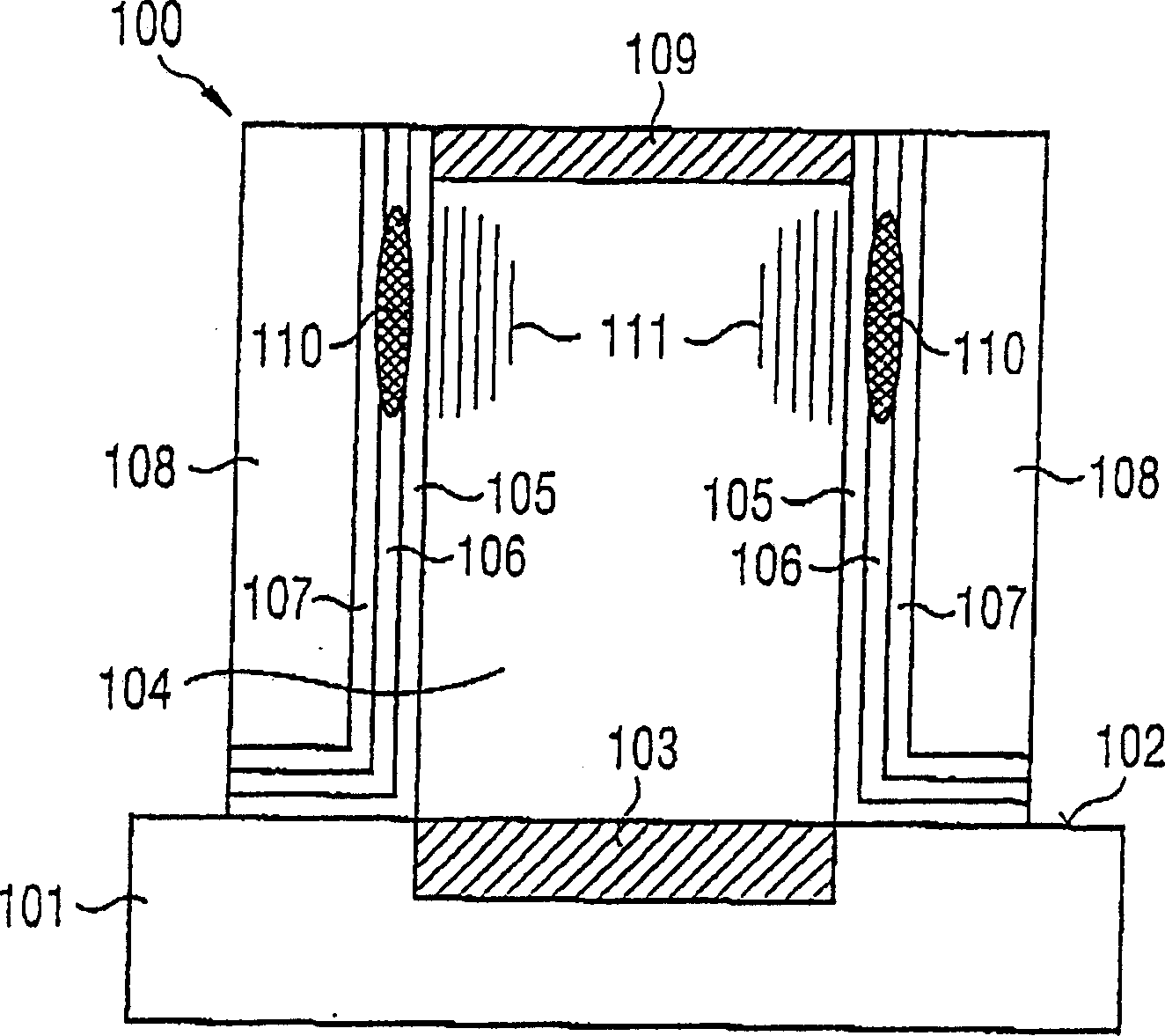
[0034] attached figure 1 A vertical cross-sectional view of a vertical transistor 100 according to an embodiment of the present invention is shown.

[0035] In the semiconductor substrate 100 made of silicon, a first bit line, which forms the source region 103 in the region of the vertical transistor, is arranged on the main side 102 . According to this exemplary embodiment, the source region 103 is produced by implanting low-ohmic dopant atoms into the semiconductor substrate 100 . According to the exemplary embodiment, arsenic atoms or phosphorus atoms are used as dopant atoms. On a device with a plurality of vertical transistors 100 in a memory matrix, the source region 103 can be used as a through-source region 103 buried in all vertical transistors 100 .

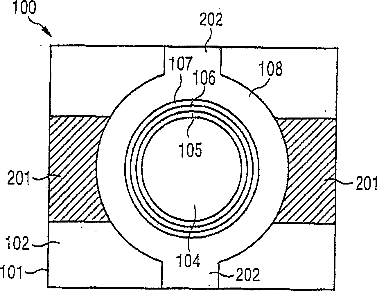
[0036] A channel region 104 arranged cylindrically symmetrically about an axis of symmetry oriented perpendicularly to main side 102 (not shown) is located on source region 103 . According to the illustrated embodime...


PUM


Abstract

A vertical transistor (100) has a source region (103), a drain region (109), a gate region (108), and a channel region (104) between the source region (103) and the drain region (109), which are arranged in a vertical direction in a semiconductor substrate (101), the gate region (104) having an electrical insulation from the source region (103), from the drain region (109) and from the channel region (104) and being arranged around the channel region (104) in such a way that the gate region (108) and the channel region (104) form a coaxial structure.

Description

technical field [0001] The present invention relates to a vertical transistor, a storage device and a method for manufacturing a vertical transistor. Background technique [0002] Due to the rapid development of computer technology, there is a need for storage media that provide larger and larger storage capacities on smaller and smaller devices. Large amounts of data are usually stored in large memory cell devices. For example, a non-volatile memory which can store stored information over a long period of time without loss of information is used as the storage unit. For example, transistors on a silicon chip can be used as non-volatile memory. [0003] But with further advancing miniaturization, conventional silicon microelectronics will run into its limits. Especially the development of ever smaller and more densely arranged transistors, with hundreds of millions of transistors per chip at the same time, will in principle encounter physical problems in the next ten year...

Claims


Application Information

Patent Timeline
Patent Type & Authority Patents(China)
IPC IPC(8): H01L29/78H01L27/105H01L21/336H01L21/28H01L29/792H10B69/00
CPCH01L29/66666H01L29/7827H01L29/66833H01L21/28282H01L29/7926H01L29/792H01L27/115H01L29/40117H10B69/00
Inventor P·哈格梅耶
Owner INFINEON TECH AG
Learn More