Check patentability & draft patents in minutes with Patsnap Eureka AI!

Nonvolatile semiconductor memory

A memory, read-only memory technology, applied in the field of stretch, non-volatile memory, which can solve the problems of high current and increased complexity

Inactive Publication Date: 2000-09-27
硅芯片公司
View PDF0 Cites 3 Cited by
  • Summary
  • Abstract
  • Description
  • Claims
  • Application Information

AI Technical Summary

Problems solved by technology

The requirement for high current adds additional complexity due to the design of high current pumps operating at low voltage

Method used


Image

  • Nonvolatile semiconductor memory
  • Nonvolatile semiconductor memory
  • Nonvolatile semiconductor memory

Examples


Embodiment Construction

[0019] Description of preferred embodiments

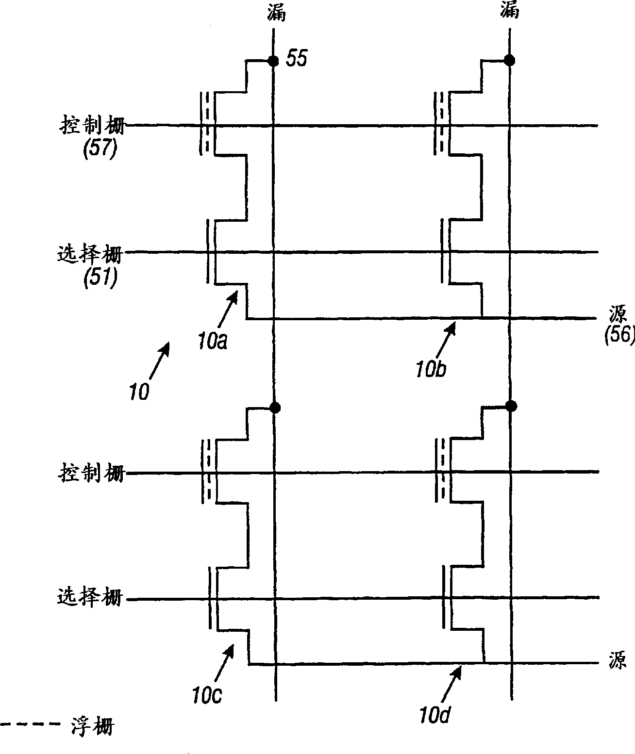
[0020] Referring to the accompanying drawings, wherein the same reference signs are used for like parts in each figure, figure 1 The illustrated memory cell 10 includes a read transistor 12 and a select transistor 14 . This structure is advantageously implemented on a semiconductor layer on which the electrically isolated floating gate 22 is arranged.

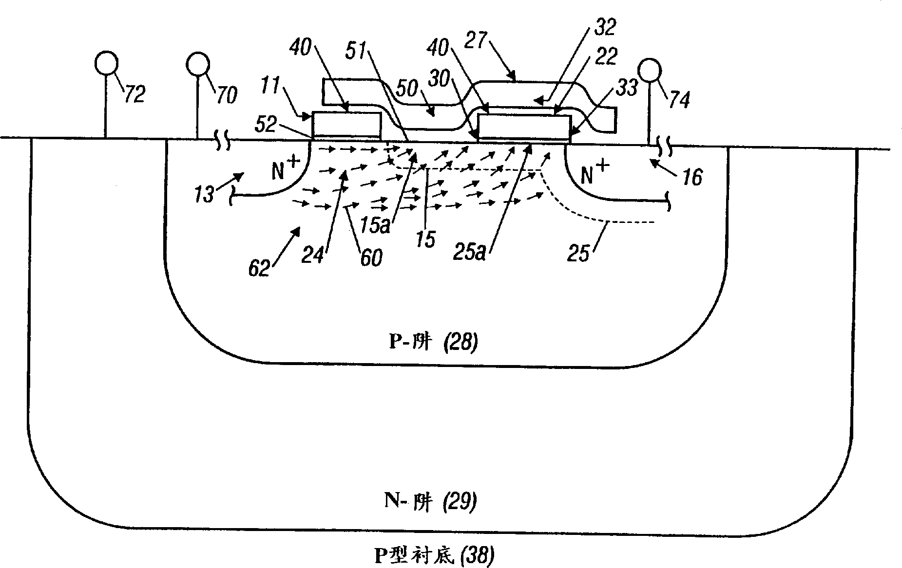
[0021] Source 13 of select transistor 14 is controlled by source node 56 for each cell 10a-10d. The gate of select transistor 11 is controlled by node 51 . The control gate 27 of the read transistor 12 is controlled by a control node 57 . Drain 16 of read transistor 12 is connected to drain node 55 .

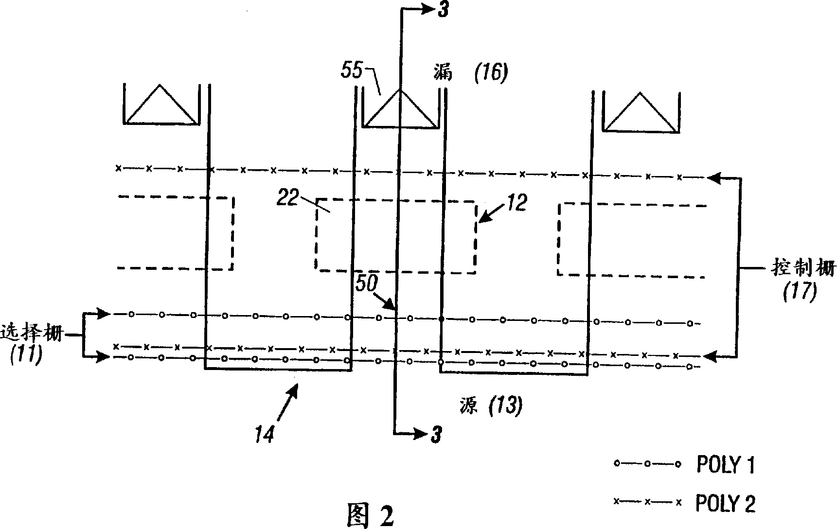
[0022] One implementation of the cell 10 layout shown in FIG. 2 includes a control gate 17 . The control gate 17 extends across an active region 18 adjacent to the drain 16 of the read transistor 12 and the source 13 of the select transistor 14 . The select gate 11 extends paral...


PUM


Abstract

A nonvolatile memory cell which is highly scalable includes a cell formed in a triple well. A select transistor can have a source which also acts as the emitter of a lateral bipolar transistor. The lateral bipolar transistor operates as a charge injector. The charge injector provides electrons for substrate hot electron injection of electrons onto the floating gate for programming. The cell depletion / inversion region may be extended by forming a capacitor as an extension of the control gate over the substrate between the source and channel of said sense transistor.

Description

Background of the invention [0001] The present invention relates generally to non-volatile memory, and more particularly to electrically erasable non-volatile memory. [0002] Non-volatile memory cells are advantageous because recorded information is retained even if power to the memory is removed. There are several different types of nonvolatile memory, including erasable programmable read-only memories (EPROMs), electrically erasable programmable read-only memories (EEPROMs), and flash (flash) EEPROM memories. EPROMs are erased by exposure, but programmed electrically using channel hot electrons injected into the floating gate. Conventional EPROMs have the same programming function, but instead of being erased by light, they can be erased and programmed by electron tunneling. In this way, information can be stored in these memories, retained when power is removed, and if required, the memories can be erased to be reprogrammed with the appropriate technology. Flash EEPROMs...

Claims


Application Information

Patent Timeline
IPC IPC(8): G11C16/04H01L21/8247H01L27/115H01L29/423H01L29/788H01L29/792
CPCH01L29/7885G11C16/0425H01L29/42328H01L27/115G11C16/0433H10B69/00G11C16/04
Inventor T·W·王
Owner 硅芯片公司
Features
  • R&D
  • Intellectual Property
  • Life Sciences
  • Materials
  • Tech Scout
  • Unparalleled Data Quality
  • Higher Quality Content
  • 60% Fewer Hallucinations
Learn More