

Digital level shifter with reduced power dissipation and false transmission blocking
A level and digital technology, applied in the field of digital level converter circuit, can solve the problems of insufficient protective increment time, long duration of transmission pulse, power loss, etc.
- Summary
- Abstract
- Description
- Claims
- Application Information
AI Technical Summary
Problems solved by technology
Method used
Image

Examples
Embodiment Construction
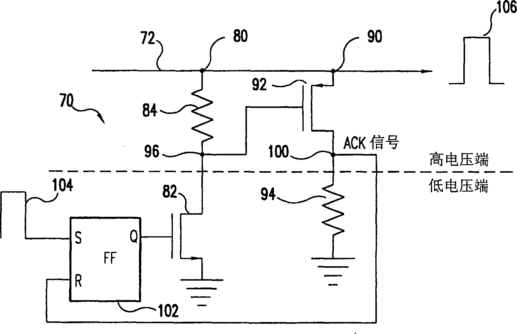
[0032] image 3 Pertinent components of the digital level shifting circuit 70 of the present invention are shown in which a feedback signal (referred to herein as an "acknowledgement" signal) is used to significantly reduce the power consumption of a level shifting device (such as a high voltage MOSFET or other suitable device) . The device is turned on and remains on until it receives an acknowledgment signal, at which point the device is turned off.
[0033] exist image 3 , circuit 70 provides a level shifted output signal on line 72, as shown in Figure 1, line 72 can provide a voltage from V OFFSET to V OFFSET +V DDH signal of change. Circuit 70 includes two current paths between line 72 and ground: in one current path, a level-shifting n-channel transistor 82 is connected in series with resistor 84 between node 80 and "ground"; , a p-channel transistor 92 is connected in series with a resistor 94 between node 90 and "ground". The gate of transistor 92 is connected be...
PUM
 Abstract
Description
Claims
Application Information