Process for plasma strengthening type chemical vapour phase deposition treatment

A technology of chemical vapor deposition and processing method, which is applied in the field of plasma-enhanced chemical vapor deposition processing, can solve problems such as dielectric breakdown, reliability failure, and surface leakage, so as to avoid the formation of bumps, improve the pass rate, The effect of eliminating defects

Active Publication Date: 2007-05-02
SEMICON MFG INT (SHANGHAI) CORP +1
View PDF5 Cites 0 Cited by
  • Summary
  • Abstract
  • Description
  • Claims
  • Application Information

AI Technical Summary

Problems solved by technology

These bumps will cover up other fatal defects and unopened vias, which may eventually lead to many defects, such as surfac

Method used


Image

  • Process for plasma strengthening type chemical vapour phase deposition treatment
  • Process for plasma strengthening type chemical vapour phase deposition treatment
  • Process for plasma strengthening type chemical vapour phase deposition treatment

Examples


Embodiment Construction

[0017] Preferred embodiments of the present invention will be described below with reference to the accompanying drawings.

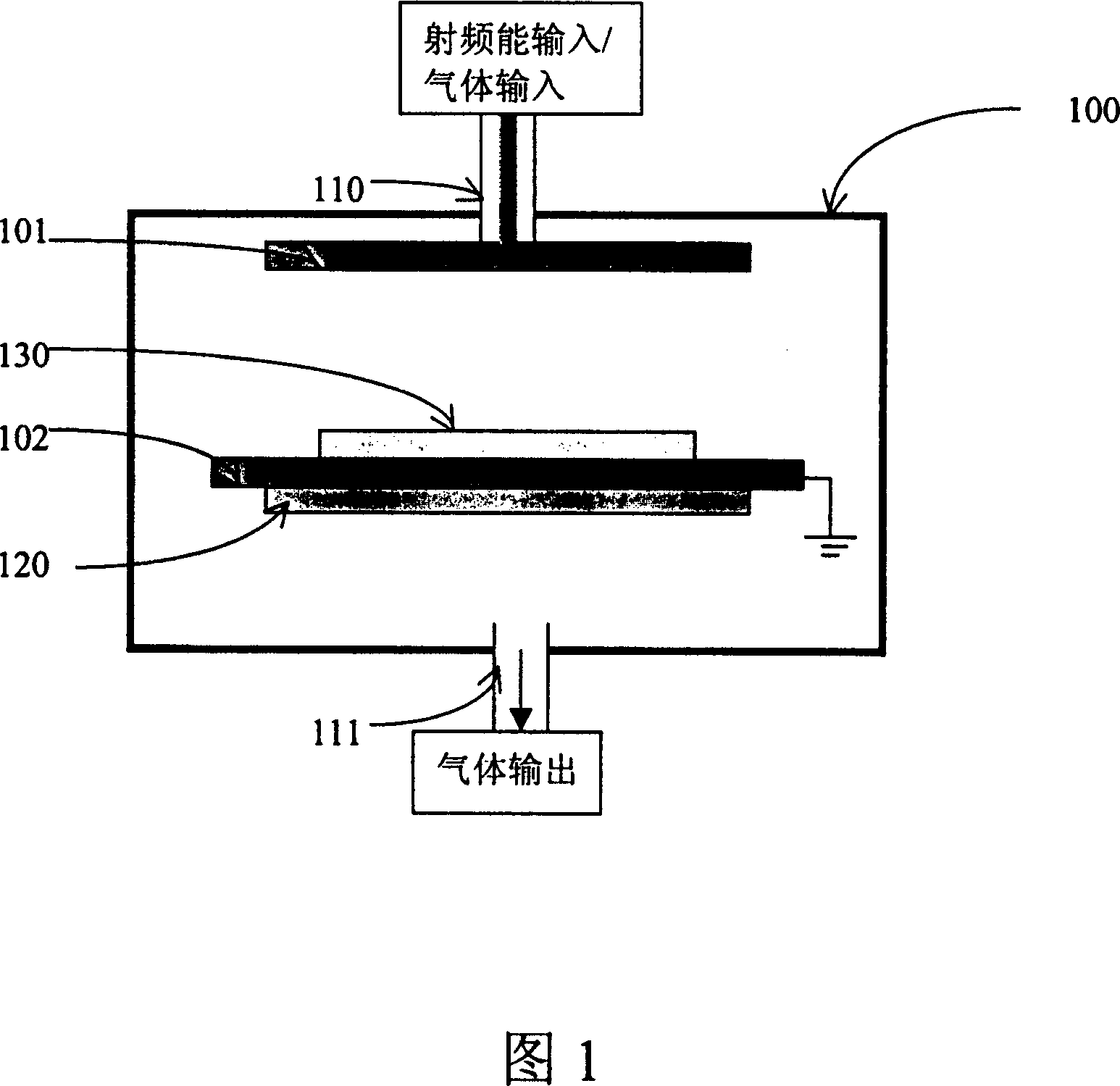
[0018] The PECVD method of the present invention still uses the reaction furnace 100 shown in FIG. 1 .

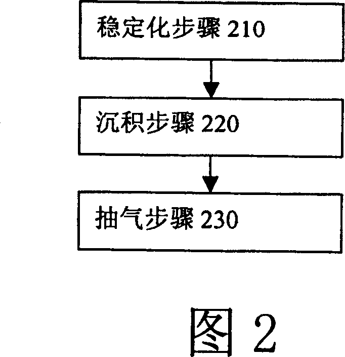
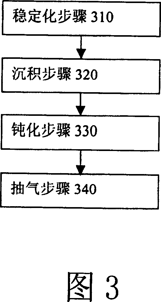
[0019] Fig. 3 is the flow chart of PECVD method according to the present invention, as can be seen by comparing Fig. 2 of traditional method, PECVD treatment method provided by the present invention has added a passivation between deposition step and pumping step with respect to traditional PECVD method transformation step. The specific steps of the PECVD method of the present invention will be described below with reference to FIG. 3 .

[0020] It can be seen from FIG. 3 that the PECVD treatment method provided by the present invention includes four steps.

[0021] First comes the stabilization step 310 . During this step, no RF energy is input. Just let the precursor gas such as NH 3 , N 2 O and N 2 , flow into the reaction furnace 100 at flo...


PUM


Abstract

The invention relates to a plasma-strengthening chemical gas phase aggradation method and is used in depositting film on the surface of the semiconductor wafer. It includes: stabilization, inputting the premonitory gas into the reaction kettle; aggradation, inputting the radio frequency energy, premonitory gas and reacton gas into the reaction kettle; passivation, stopping inputting the reaction gas but still inputting the readio frequency energy; and air bleeding, turning off the radio frequency energy, stopping inputting the premonitory gas and pumping the remaining gas out of the reaction kettle. During the passivation, the radio frequency energy is same with or less than that in the aggradation and we still input the premonitory gas for 3 to 15 minutes. Because the invention adds the passivation to it makes the Si which does not react with other on the surface of the wafer continue reacting till the end, it can eliminate the incomplete surface reaction and hanging keys, thus avoids the protuberant block in the film, eliminates the disadvantage and increases the yield.

Description

technical field [0001] The invention relates to the technical field of semiconductor manufacturing, in particular to a plasma-enhanced chemical vapor deposition (PECVD) treatment method. Background technique [0002] In the semiconductor manufacturing process, in order to make discrete devices and integrated circuits, different types of thin films need to be deposited on the wafer substrate. Among methods for depositing thin films, plasma enhanced chemical vapor deposition (PECVD, Plasma Enhanced Chemical Vapor Deposition) is a commonly used method. The method uses energy to enhance the CVD reaction, and in addition to the thermal energy of the general CVD system, additional plasma energy is added. [0003] FIG. 1 shows a schematic diagram of a common device for PECVD method, and the PECVD device is a PECVD reactor. As shown in FIG. 1 , the reaction furnace 100 is made of cylindrical glass or aluminum, and the upper and lower ends are sealed with aluminum plates. There ar...

Claims


Application Information

Patent Timeline
IPC IPC(8): C23C16/505
Inventor 汪钉崇
Owner SEMICON MFG INT (SHANGHAI) CORP
Why Eureka
Try Eureka