

Method and apparatus for power amplification
A technology for power amplification and input power, applied in power amplifiers, parts of amplifying devices, improving amplifiers to improve efficiency, etc., can solve problems such as large power consumption, complex feedback control circuits, and increased hardware scale
- Summary
- Abstract
- Description
- Claims
- Application Information
AI Technical Summary
Problems solved by technology
Method used
Image

Examples
Embodiment 1
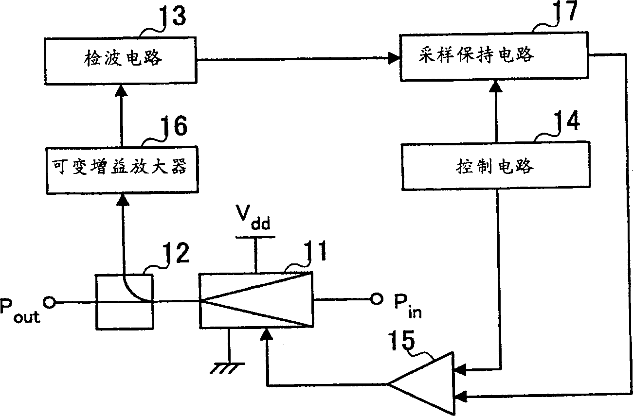
[0030] In Embodiment 1 of the present invention, a gain / bias amplifier is provided in the power amplification device, and the detection voltage is converted into a desired voltage value as the gate voltage of the power amplifier.
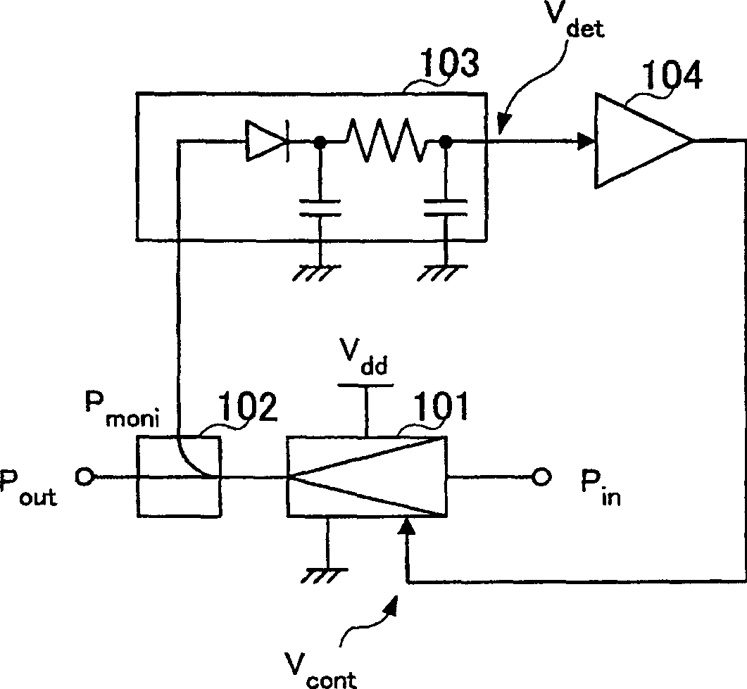
[0031] figure 2 A block diagram of main parts showing a schematic configuration of a power amplifying device according to Embodiment 1 of the present invention.
[0032] exist figure 2 Among them, the power amplifier 101 has at least one current control terminal (for example, a gate terminal of FET), and amplifies high-frequency signals. The coupler 102 monitors the amplified signal power P of the power amplifier 101 moni .
[0033] The detector 103 is an envelope detector composed of diodes, capacitors, resistors, etc., for a certain input voltage (for example, P moni >-5dBm) for linear half-wave rectification, integrated by RC filter to generate detection voltage V det .
[0034] Gain / bias amplifier 104 detects the voltage V det At least ...
Embodiment 2
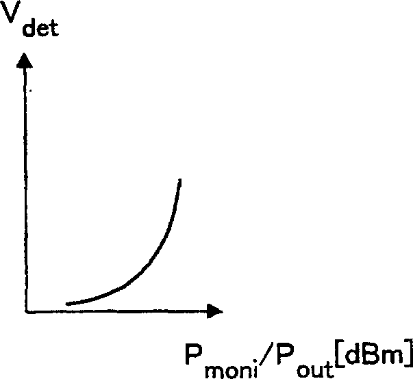
[0043] Among them, if the amplitude provided by the forward voltage is large enough (high power), the detection can be sufficiently performed in the linear region, but when the amplitude is small (low power), it becomes the nonlinear region of the diode. For detection, envelope detection may not be possible because a sufficient detection voltage cannot be generated.
[0044] Embodiment 2 of the present invention is to solve this problem. In a power amplifying device having the same structure as Embodiment 1, a bias voltage is applied to the positive terminal of the detection diode.
[0045] Figure 4 A block diagram of main parts showing a schematic configuration of the power amplifying device of this embodiment. again, in Figure 4 in, where and figure 2 The same structures are assigned the same symbols, and detailed description thereof will be omitted.
[0046] Such as Figure 4 As shown, in this embodiment, a new diode 301 is connected to the positive terminal of the ...
Embodiment 3
[0051] Among them, generally speaking, the input power is handled by the absolute value representation [dBm] using the logarithm. The diode used in the detector 103 has a linear detection characteristic, and if the detection input power is considered in absolute value [dBm], there is also a logarithmic characteristic between the input power and the detection voltage.
[0052] Furthermore, when the current control of the power amplifier is performed, if the logarithmic characteristic is maintained, the detection voltage characteristic at low power is approximately constant, making it difficult to perform current reduction control.
[0053] Embodiment 3 of the present invention is to solve this problem. In a power amplifying device having the same structure as Embodiment 1, an offset circuit and a logarithmic amplifier are provided at the output end of the detection diode to convert the detection voltage characteristic into a linear characteristic.
[0054] Figure 6 A block di...
PUM
 Abstract
Description
Claims
Application Information