Light conducting plate and manufacturing method thereof

A manufacturing method and technology of a light guide plate, applied in the direction of copying/marking method, optics, nonlinear optics, etc., can solve the problems of increasing the overall thickness of the backlight module 100, increasing the process time and cost, light leakage, etc., achieving high reproducibility and simplification Process and cost, the effect of reducing the possibility of light leakage

Active Publication Date: 2007-05-16
AU OPTRONICS CORP
View PDF8 Cites 0 Cited by
  • Summary
  • Abstract
  • Description
  • Claims
  • Application Information

AI Technical Summary

Problems solved by technology

However, attaching the reflective sheet 130 not only increases the process time and cost, but also increases the overall thickness of the backlight module 100
Moreover, even after the reflective sheets 130 are attached to surfaces other than the light incident surface S1 and the light exit surface S3 of the light guide plate 110, the light guide plate 110 still has the possibility of light leakage at the joints of the reflective sheets 130.
Therefore, for liquid crystal displays that are developing towards ultra-high brightness and ultra-thin size, there are still many shortcomings to be overcome in the existing conventional light guide plate manufacturing methods
[0008] It can be seen that the above-mentioned existing light guide plate and its manufacturing method obviously still have inconvenience and defects in structure, manufacturing method and use, and need to be further improved urgently.
In order to solve the problems existing in the light guide plate and its manufacturing method, the relevant manufacturers have tried their best to find a solution, but no suitable design has been developed for a long time, and there is no suitable structure for general products to solve the above problems , this is obviously a problem that relevant industry players are eager to solve

Method used


Image

  • Light conducting plate and manufacturing method thereof
  • Light conducting plate and manufacturing method thereof
  • Light conducting plate and manufacturing method thereof

Examples


Embodiment Construction

[0057] In order to further explain the technical means and effects of the present invention to achieve the intended purpose of the invention, the specific implementation, structure and manufacturing method of the light guide plate and its manufacturing method proposed according to the present invention will be described below in conjunction with the accompanying drawings and preferred embodiments. , steps, features and effects thereof are described in detail below.

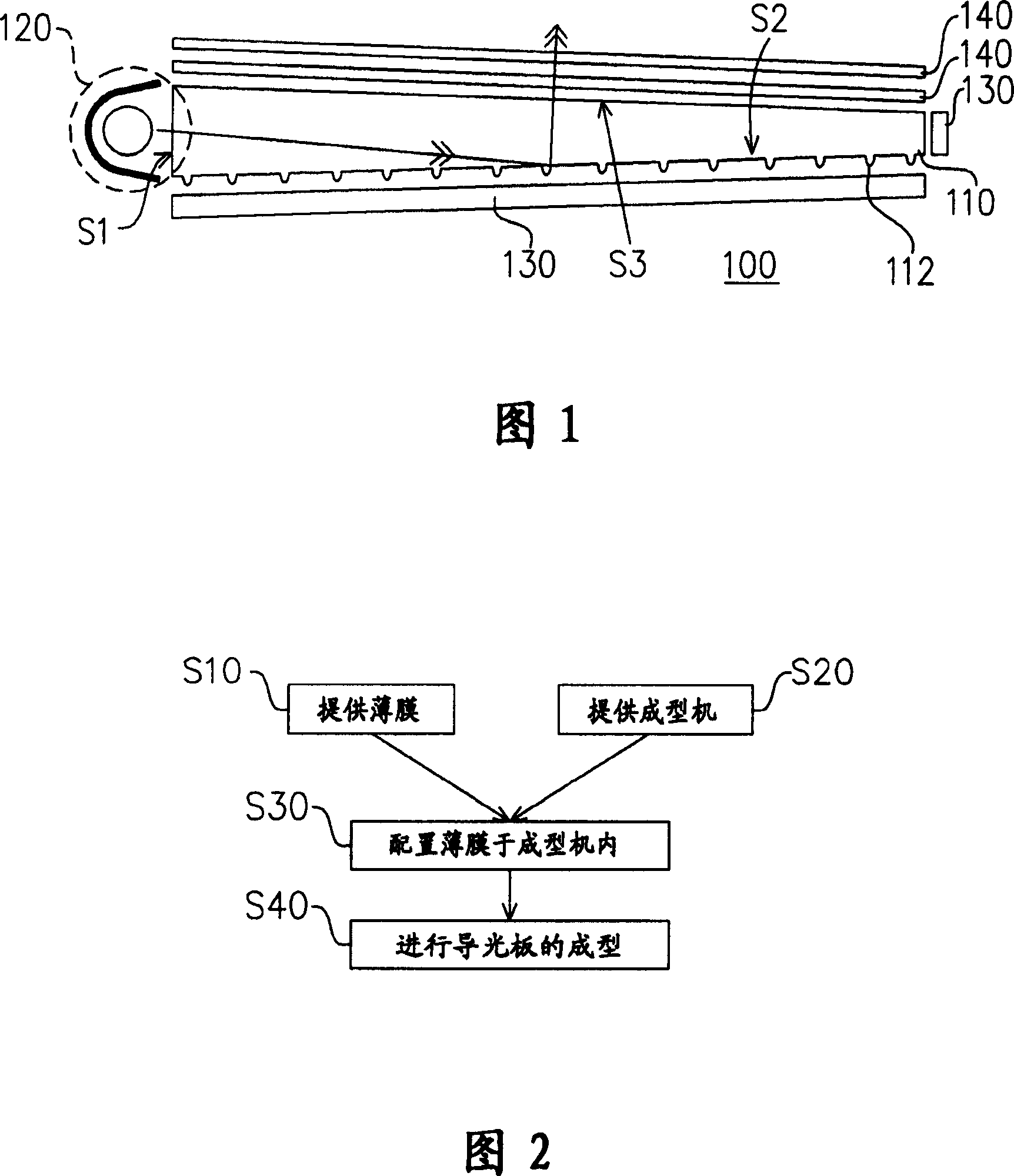
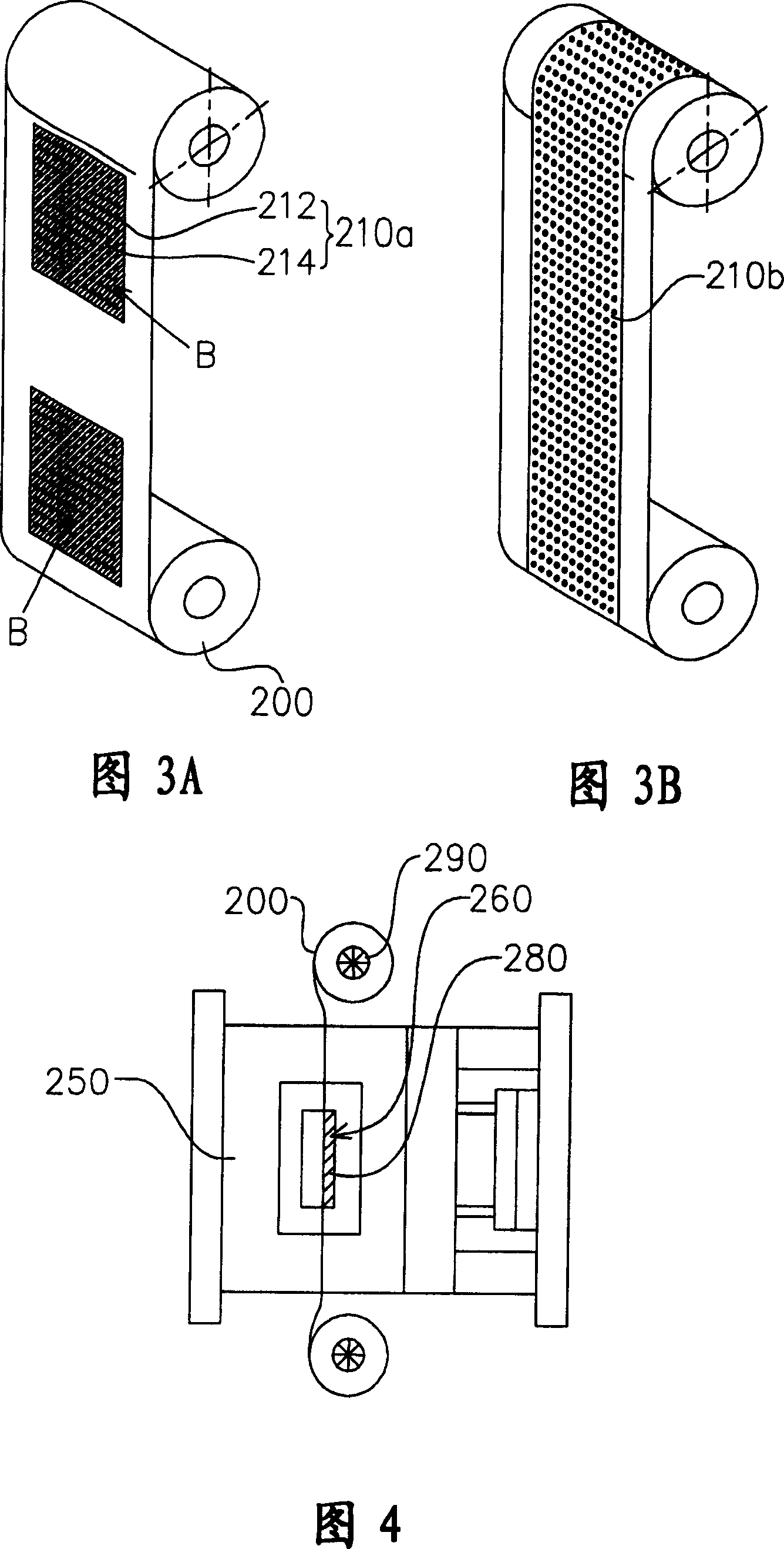
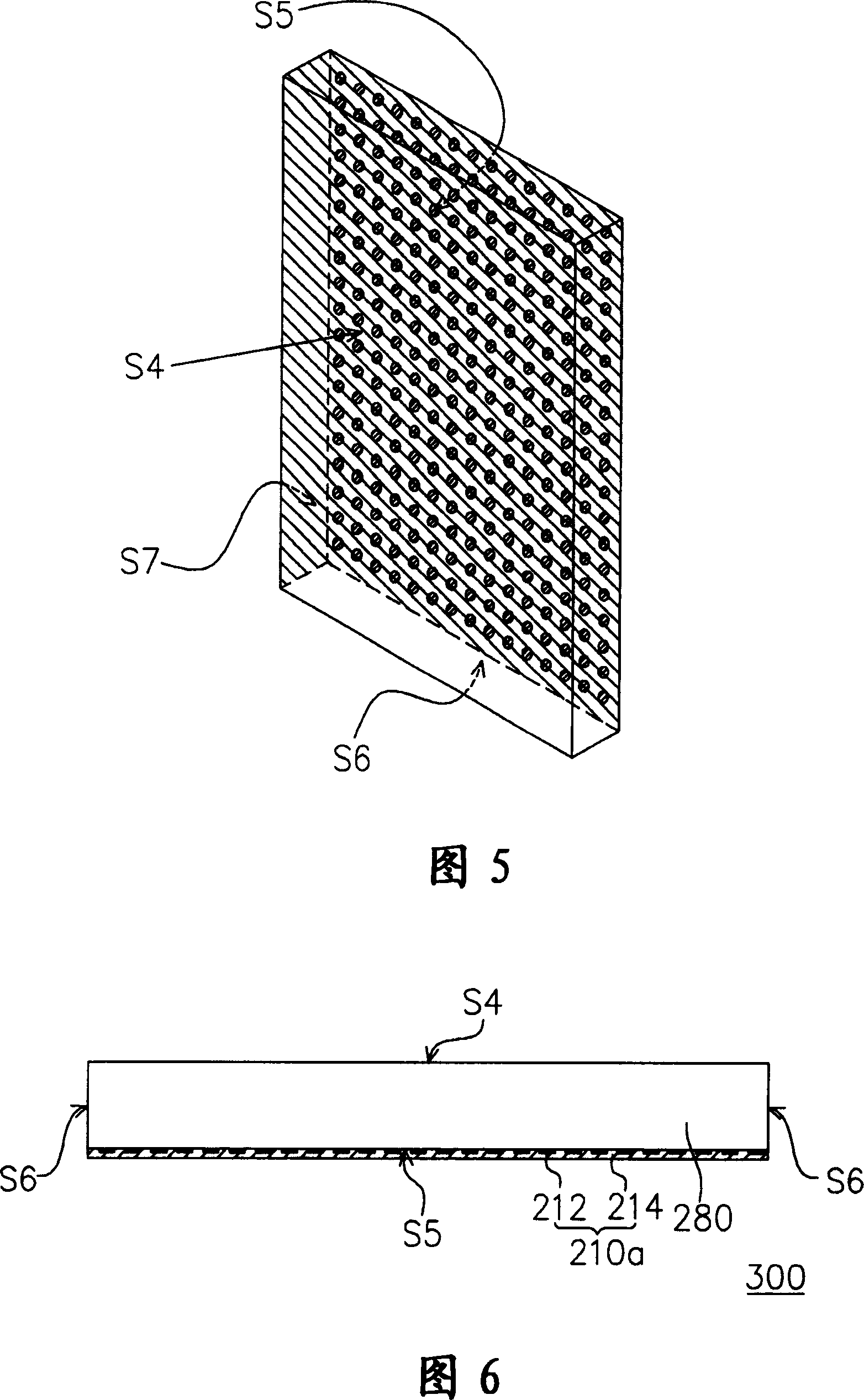
[0058] Please refer to FIG. 2 , which is a flow chart of manufacturing a light guide plate according to a preferred embodiment of the present invention, and FIG. 3A and FIG. 3B are schematic diagrams of two kinds of tape-and-roll films used in the present invention.

[0059] Please refer to FIG. 2 and FIG. 3A , the manufacturing method of the light guide plate of the present invention is to provide a film 200 with a transfer material layer 210 a on the film 200 (step S10 ). The film 200 is, for example, a roll fil...


PUM


Abstract

This invention relates to a manufacturing method of light conducting board including steps that follows: first to provide a thin film with a transfer- printing material coat, and then to provide a light conductive plate shaper with nest in, later to locate a thin film in the shaper and locate part of transfer-printing material in the nest, finally to put a forming light conductive plate in the module nest. The above transfer-printing material coat is in the light conductive plate. The preparation method of light conductive plate in this method can improve the replicability of the light conductive plate and reduce the thickness of the plate and decrease the possibility of light leaking of the plate.

Description

technical field [0001] The present invention relates to a light guide and a manufacturing method thereof, in particular to a light guide using transfer printing technology and a manufacturing method thereof. Background technique [0002] The rapid progress of the multimedia society is mostly due to the rapid progress of semiconductor components or man-machine display devices. As far as the display is concerned, the cathode ray tube (Cathode Ray Tube, CRT) has been monopolizing the display market in recent years due to its excellent display quality and economy. However, for the environment where most of the personal operations are terminals / display devices, if we cut in from the viewpoint of environmental protection, or predict the trend of saving energy, there are still many problems in the use of space and energy consumption of cathode ray tubes. However, there is no effective solution to the requirements of lightness, thinness, shortness, smallness and low power consumpti...

Claims


Application Information

Patent Timeline
Patent Type & Authority Patents(China)
IPC IPC(8): G02F1/1335B41M5/035
Inventor 郑世明
Owner AU OPTRONICS CORP
Why Eureka
Try Eureka