Structure and method for preventing micro image processing aligning mistake

A process and lithography technology, applied in the direction of electrical components, semiconductor/solid-state device manufacturing, circuits, etc., can solve problems such as misalignment, component pattern offset, etc., and achieve the effect of reducing stress and improving deposition uniformity

Inactive Publication Date: 2007-07-04
MACRONIX INT CO LTD
View PDF3 Cites 2 Cited by
  • Summary
  • Abstract
  • Description
  • Claims
  • Application Information

AI Technical Summary

Problems solved by technology

In other words, if the alignment marks 130a are used to align the mask during the subsequent lithography process, misalignment will occur, which will cause device patterns to deviate.

Method used


Image

  • Structure and method for preventing micro image processing aligning mistake
  • Structure and method for preventing micro image processing aligning mistake
  • Structure and method for preventing micro image processing aligning mistake

Examples


Embodiment Construction

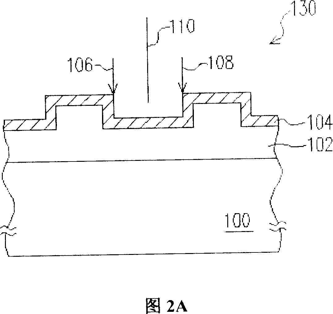
[0034] FIG. 3 is a schematic cross-sectional view of an alignment mark according to a preferred embodiment of the present invention, and FIG. 4 is an enlarged view at 300 in FIG. 3 . 3 and 4, an anti-electromigration layer 302 is formed on the structural layer 102 above the substrate 100, and then a conductive layer 104 is formed on the anti-electromigration layer 302, and a conductive layer 104 is formed on the conductive layer 104. anti-reflection layer 304 , so that the conductive layer 104 is sandwiched between the anti-electromigration layer 302 and the anti-reflection layer 304 . It is particularly worth mentioning that the anti-reflection layer 304 also has the functions of resisting electromigration and serving as the end point of the etching process.

[0035] In a preferred embodiment, the substrate 100 is, for example, a silicon substrate, and the structural layer 102 is, for example, a patterned dielectric layer. The conductive layer 104 is, for example, an aluminu...


PUM


Abstract

A structure and method for preventing the aligning error in micropattern process of internal metal wire are disclosed. Said method includes generating an aluminium layer on the structure layer of substrate, and generating an anti-reflection layer consisting of at least two Ti layers and at least two titanium nitride layers, which are alternatively laminated in order to disperse the stress of titanium nitride for preventing the generation of aligning error in following steps.

Description

technical field [0001] The present invention relates to a structure and method for preventing misalignment in lithography process, and in particular to a structure and method for preventing misalignment in lithography process of metal interconnection. Background technique [0002] With the advancement of semiconductor technology, the size of components is also continuously reduced. When the integration of integrated circuits increases, so that the surface of the chip cannot provide enough area to make the required interconnection, in order to meet the increased interconnection requirements after the shrinkage of components, multilayer metal interconnections with more than two layers The design of the VLSI technology has become the way that must be adopted in the very large scale integration (VLSI) technology. [0003] Usually, when defining each metal interconnection layer, the alignment marks designed on the edge of the wafer are used to align the photomask, so that there ...

Claims


Application Information

Patent Timeline
Patent Type & Authority Patents(China)
IPC IPC(8): H01L21/768H01L21/3205
Inventor 苏金达赖隽仁颜裕林
Owner MACRONIX INT CO LTD
Why Eureka
Try Eureka