

Chip conducting lug and re-distributed wire layer configuration
A conductive bump and redistribution technology, applied in circuits, electrical components, electrical solid devices, etc., can solve the problems of poor speed performance, high impedance, and difficulty in increasing the density of conductive bumps, reducing resistance value and increasing intersection. the effect of the probability of
- Summary
- Abstract
- Description
- Claims
- Application Information
AI Technical Summary
Problems solved by technology
Method used
Image

Examples
Embodiment Construction
[0045] The preferred embodiment of the present invention will be described in more detail with the help of the following figures in the following explanatory text:
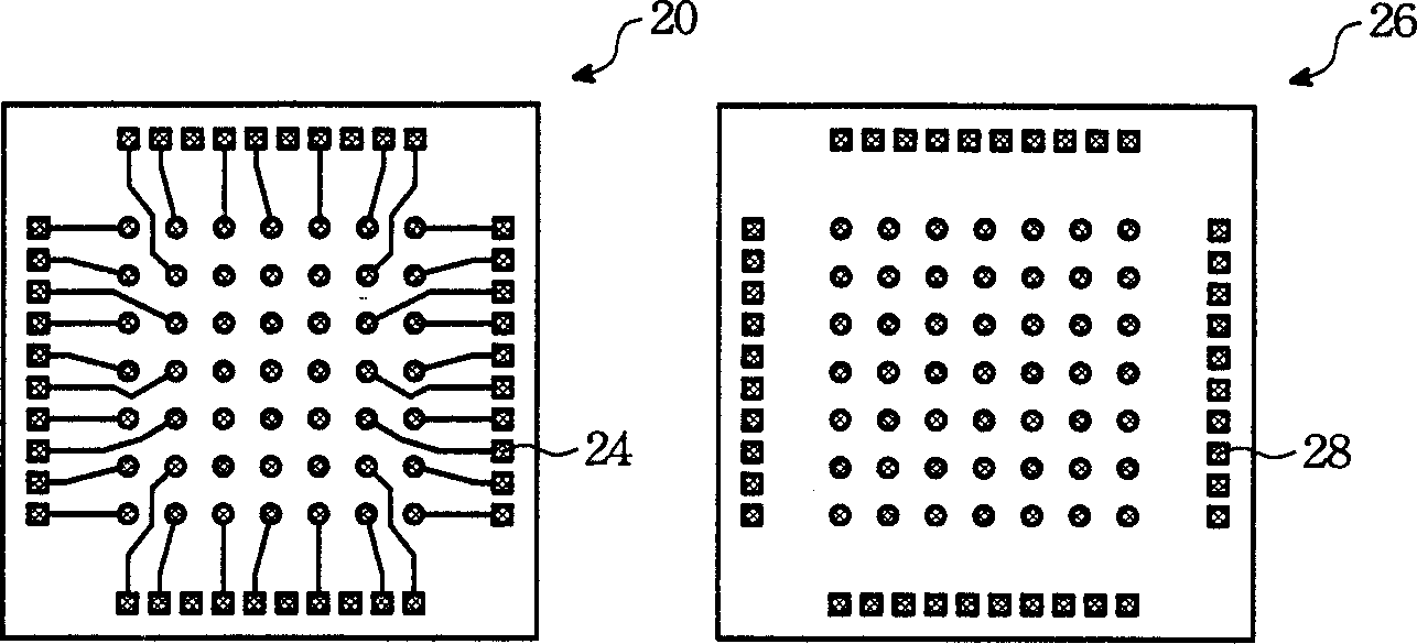
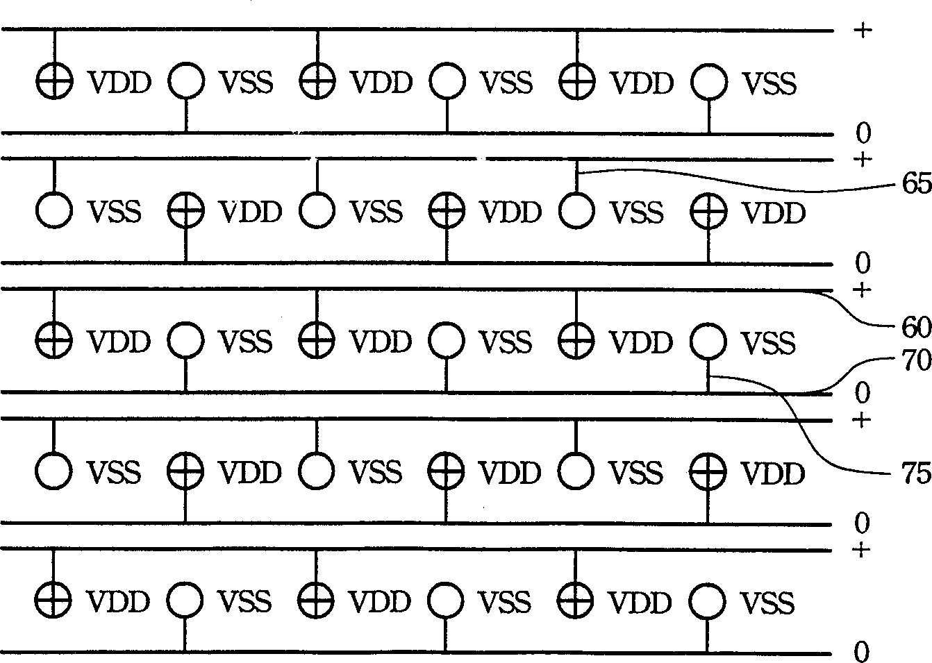
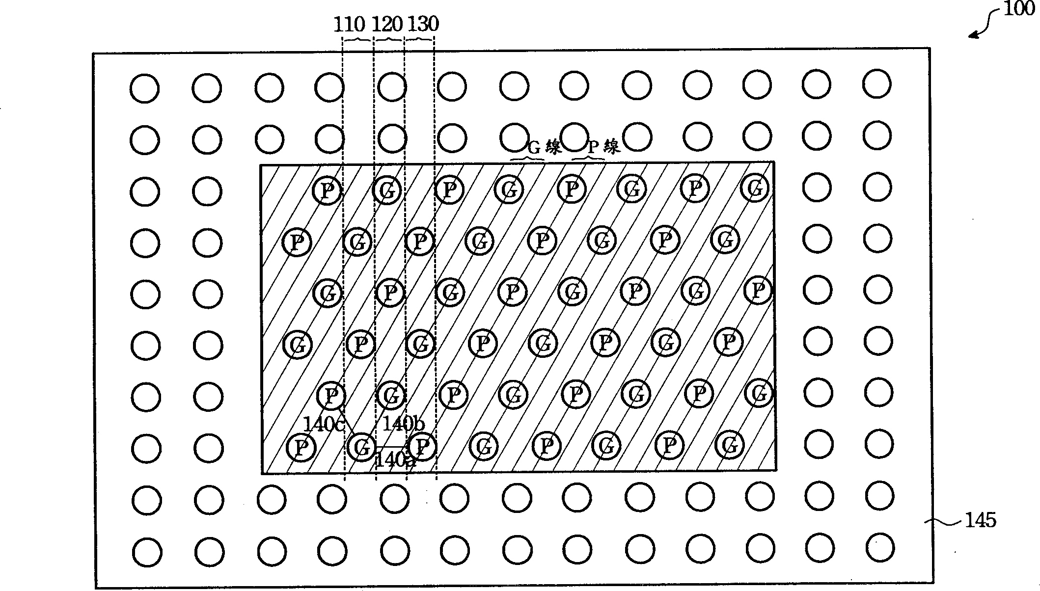
[0046] The method provided by the invention, such as image 3 A schematic diagram of the first embodiment is shown. The common arrangement of conductive bumps arranged in an array at the core position of the flip-chip chip in the traditional method is changed to a row-to-row staggered arrangement. In addition, all signal conductive bumps have been moved to the periphery of the chip (not shown). The chip core 100 only has the voltage source conductive bump P and the ground conductive bump G.
[0047] still as image 3 , the conductive bumps listed in the marked row 120 and the conductive bumps listed in the left adjacent vertical row 110 and the right adjacent vertical row 130 are alternately arranged. Moreover, the voltage source conductive bumps P and the ground conductive bumps G in each vertical row are also...
PUM
 Abstract
Description
Claims
Application Information