Packing of memory device using electron emitting
A technology of emitters and electron beams, applied in the direction of electric solid-state devices, static memory, digital memory information, etc., can solve problems such as impact, electron beam dispersion, and difficulties
- Summary
- Abstract
- Description
- Claims
- Application Information
AI Technical Summary
Problems solved by technology
Method used
Image
Examples
Embodiment Construction
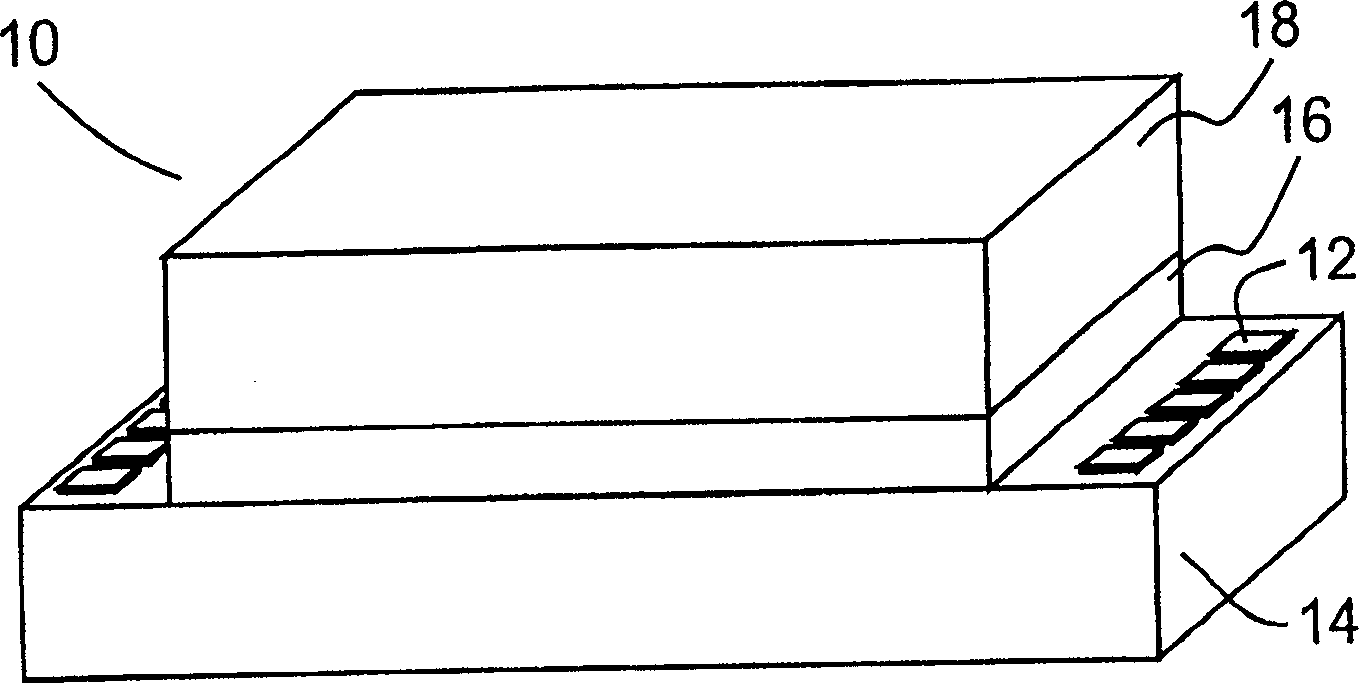
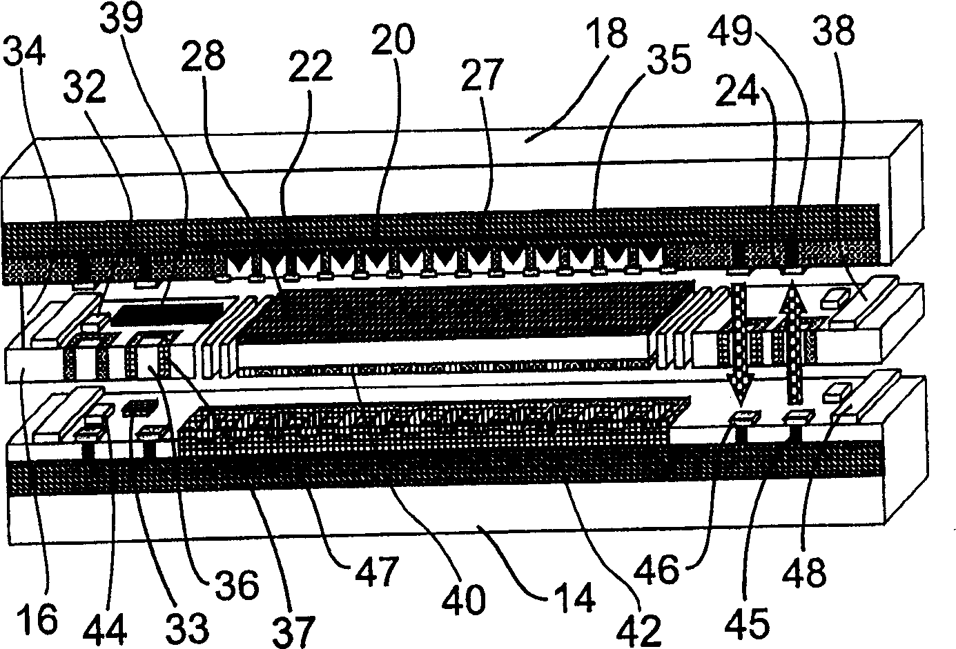
[0022] refer to figure 1 , where an atomic resolution memory component of a preferred embodiment of the present invention is shown. Atomic Resolution Storage, or ARS, as used herein, refers to storage and retrieval of information where the storage medium supports greater than 100 gigabits per square inch and the electron beam is focused by electron optics. It is preferred, but not necessary, to use sophisticated MEMS motors to access areas of the storage medium; scanning the electron beam may also accomplish the same.
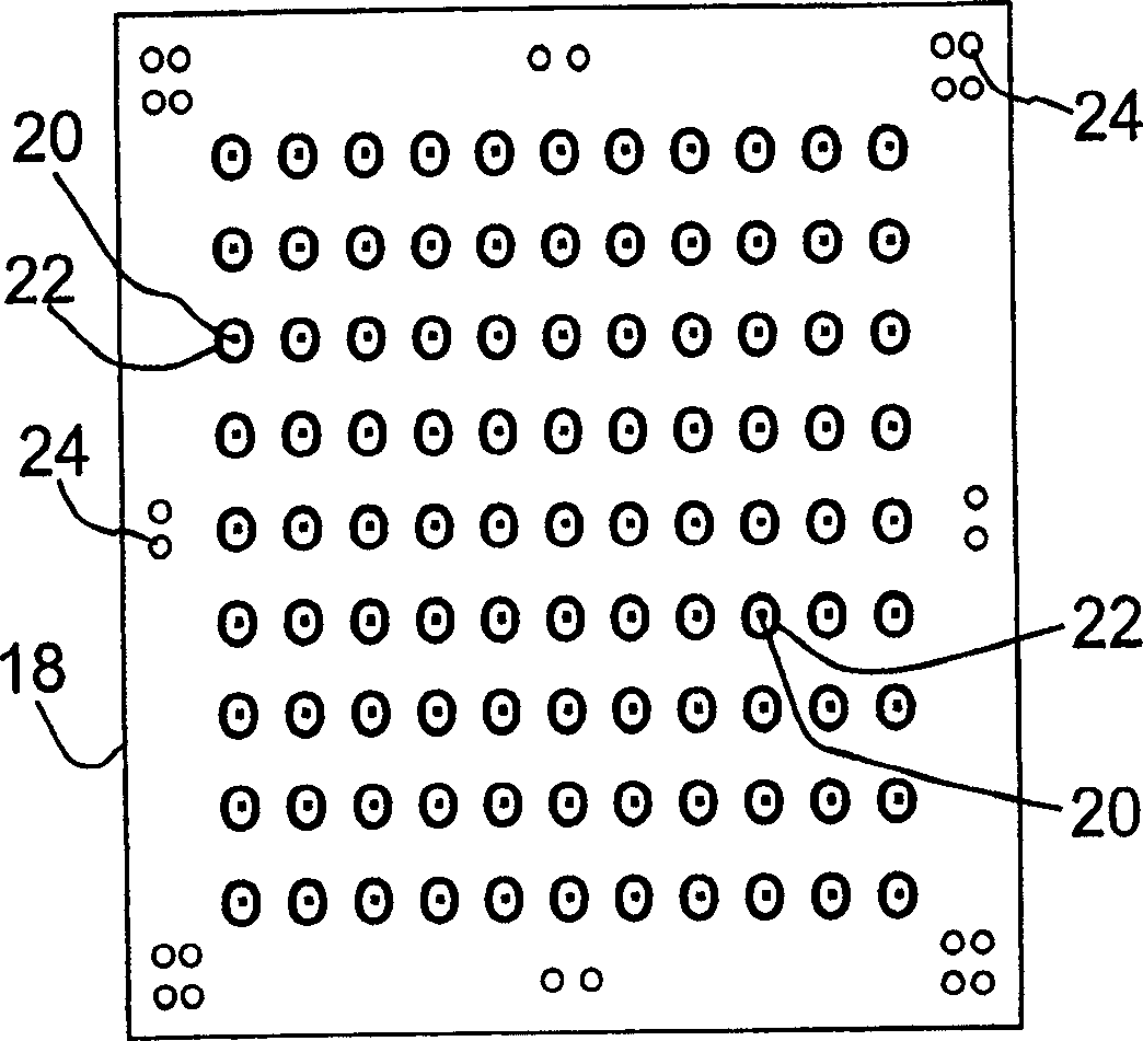
[0023] figure 1 Shown is an assembled ARS module or module 10 having tabs 12 for connection to external circuitry. The module 10 comprises 3 stacked wafers, a stator wafer N, a rotor wafer 16 and an emitter wafer 18 . The wafers are preferably fabricated by standard semiconductor and MEMS microfabrication processes and have approximately the same X-Y dimensions. The ARS assembly 10 is preferably vacuum-sealed, with the wafers spaced apart and bonded togethe...
PUM
 Abstract
Description
Claims
Application Information
 - R&D
- Intellectual Property
- Life Sciences
- Materials
- Tech Scout
- Unparalleled Data Quality
- Higher Quality Content
- 60% Fewer Hallucinations
Browse by: Latest US Patents, China's latest patents, Technical Efficacy Thesaurus, Application Domain, Technology Topic, Popular Technical Reports.
© 2025 PatSnap. All rights reserved.Legal|Privacy policy|Modern Slavery Act Transparency Statement|Sitemap|About US| Contact US: help@patsnap.com


