Active array type display apparatus

A display device and an active matrix technology, which is applied in the field of active matrix organic electro-display devices, and can solve problems such as complex wiring methods, decreased pass rate, and decreased aperture ratio.

Inactive Publication Date: 2002-10-23
SONY CORP
View PDF0 Cites 49 Cited by
  • Summary
  • Abstract
  • Description
  • Claims
  • Application Information

AI Technical Summary

Problems solved by technology

Correspondingly, the design of scanning lines and signal lines should be bent along the sub-pixel arrangement direction, resulting in complicated wiring methods
Many bends in wiring increases susceptibility to faults, leading to poor yield
In addition, in some wiring layouts, the wiring crosses the sub-pixels, which leads to a decrease in the aperture ratio

Method used


Image

  • Active array type display apparatus
  • Active array type display apparatus
  • Active array type display apparatus

Examples


Embodiment Construction

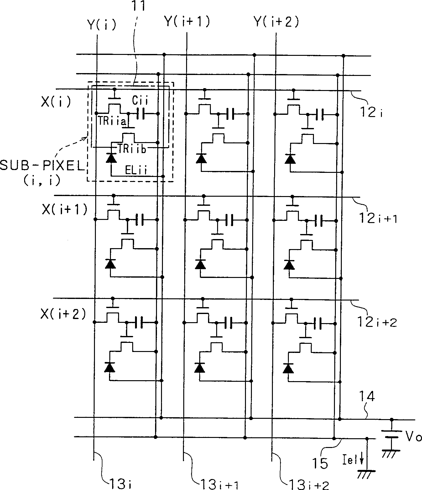
[0033] The preferred embodiments of the present invention will be described in detail below according to the accompanying drawings. image 3 It is a circuit diagram for illustrating an active matrix type display device, such as an active matrix type organic EL display device, according to an embodiment of the present invention.

[0034] exist image 3 In the present invention, a large number of sub-pixel circuits (hereinafter referred to as sub-pixels) 11 are distributed in a matrix to form a display area. In this case, to simplify the figure, only three rows of sub-pixel structures from i to i+2 and three columns from i to i+2 are shown. This display area provides scan lines l2i to l2i+2 for the sub-pixel circuit 11, and they are successively added to scan signals 2X(i) to X(i+2), so each sub-pixel can be selected by row unit; at the same time Data lines (signal lines) 13i and 13i+2 are also provided, which provide sub-pixels with pieces of image data such as luminance data...


PUM


Abstract

In the active matrix type display device according to the present invention, the device layer (light-emitting part) is formed by arranging the light-emitting part in sub-pixel units, and the circuit layer (sub-pixel circuit) is formed by driving the light-emitting part The sub-pixel circuit is arranged in the sub-pixel unit. When the device layer and the circuit layer are stacked on the substrate, the following method is proposed: the device uses the strip structure as the structure of the sub-pixel circuit, and the Δ The structure acts as the light-emitting part of the structure. Therefore, the reliability of the sub-pixel circuit can be improved when the advantage of the delta structure is utilized in the light emitting portion, thus achieving high reliability, high resolution and high brightness of the display device.

Description

technical field [0001] The present invention relates to an active matrix type display device that controls display by a sub-pixel unit by utilizing an active device provided for each sub-pixel, and particularly relates to an electroluminescent device using an organic material (hereinafter referred to as an organic EL device) An active matrix type organic electroluminescence display device as a light emitting device (electro-optic device) for each sub-pixel. Background technique [0002] Recently, an organic EL display device using an organic EL device as a light emitting device provided for each sub-pixel has attracted attention as a flat panel display. An organic EL device has a structure in which an organic material is sandwiched between two electrodes, an anode and a cathode. When a voltage is applied between the two electrodes, electrons are emitted from the cathode to the organic layer, and holes are emitted from the anode to the organic layer, where the electrons and ...

Claims


Application Information

Patent Timeline
Patent Type & Authority Applications(China)
IPC IPC(8): H05B33/12G02F1/133G09F9/30G09G3/20G09G3/30G09G3/32H01L27/32H01L51/50
CPCG09G3/3233G09G2300/0452G09G2300/0804G09G2300/0814G09G2300/0842H10K59/35H10K59/121H10K59/123G02F1/133
Inventor 浅野慎山田二郎森敬郎关谷光信
Owner SONY CORP
Why Eureka
Try Eureka