Imaging display panel and imaging observation device therewith

An image display panel and image display technology, applied in the field of image observers, can solve the problems of increasing the manufacturing cost of image display devices, etc.

Inactive Publication Date: 2003-01-15
JAPAN DISPLAY INC
View PDF0 Cites 7 Cited by
  • Summary
  • Abstract
  • Description
  • Claims
  • Application Information

AI Technical Summary

Problems solved by technology

In this high-voltage power supply circuit part, since it is necessary to use high withstand voltage components other than ordinary LSI, it is difficult to form all the peripheral devices with ordinary low withstand voltage LSI, thereby increasing the manufacturing cost of the image display device.

Method used


Image

  • Imaging display panel and imaging observation device therewith
  • Imaging display panel and imaging observation device therewith
  • Imaging display panel and imaging observation device therewith

Examples


Embodiment 1

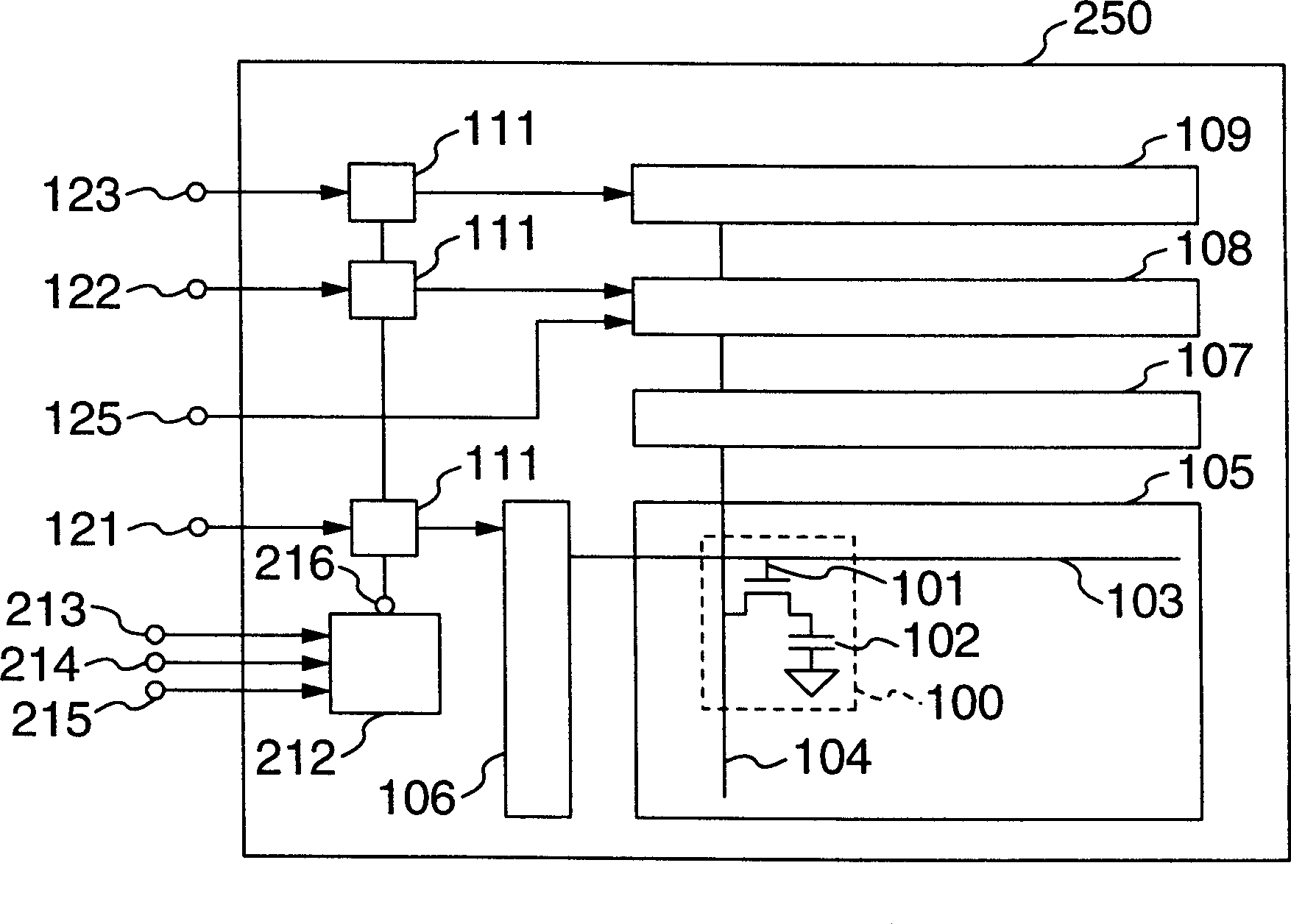
[0019] figure 1 It is a structural diagram of the image display panel 250 of this embodiment.

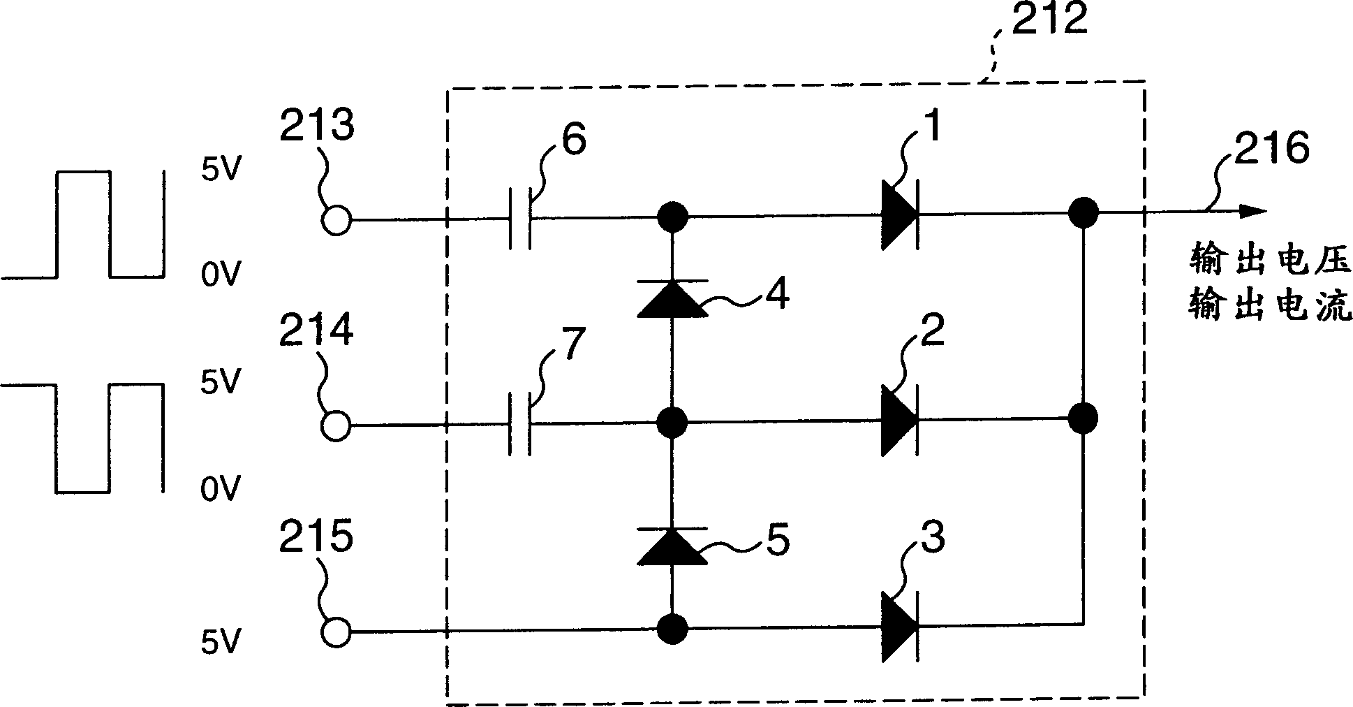
[0020] The main structure and operation of the image display panel 250 of this embodiment are similar to those already described. Figure 7 The previous example is the same, so its description is omitted. in figure 1 Middle and Figure 7 The same symbols indicate the same constituent elements. The feature of this embodiment when compared with the above-mentioned conventional example is that a high voltage generating circuit 212 for supplying a high voltage to each level shift circuit 111 is provided. That is, in order to supply a high voltage to each level shift circuit 111, a high voltage generating circuit 212 is provided, and a clock with a predetermined frequency of 5V amplitude is input from the high voltage generating circuit input terminals 213 and 214, and a constant voltage input terminal 215 is input. A constant voltage of 5V is supplied to each level shift circuit 111 from...

Embodiment 2

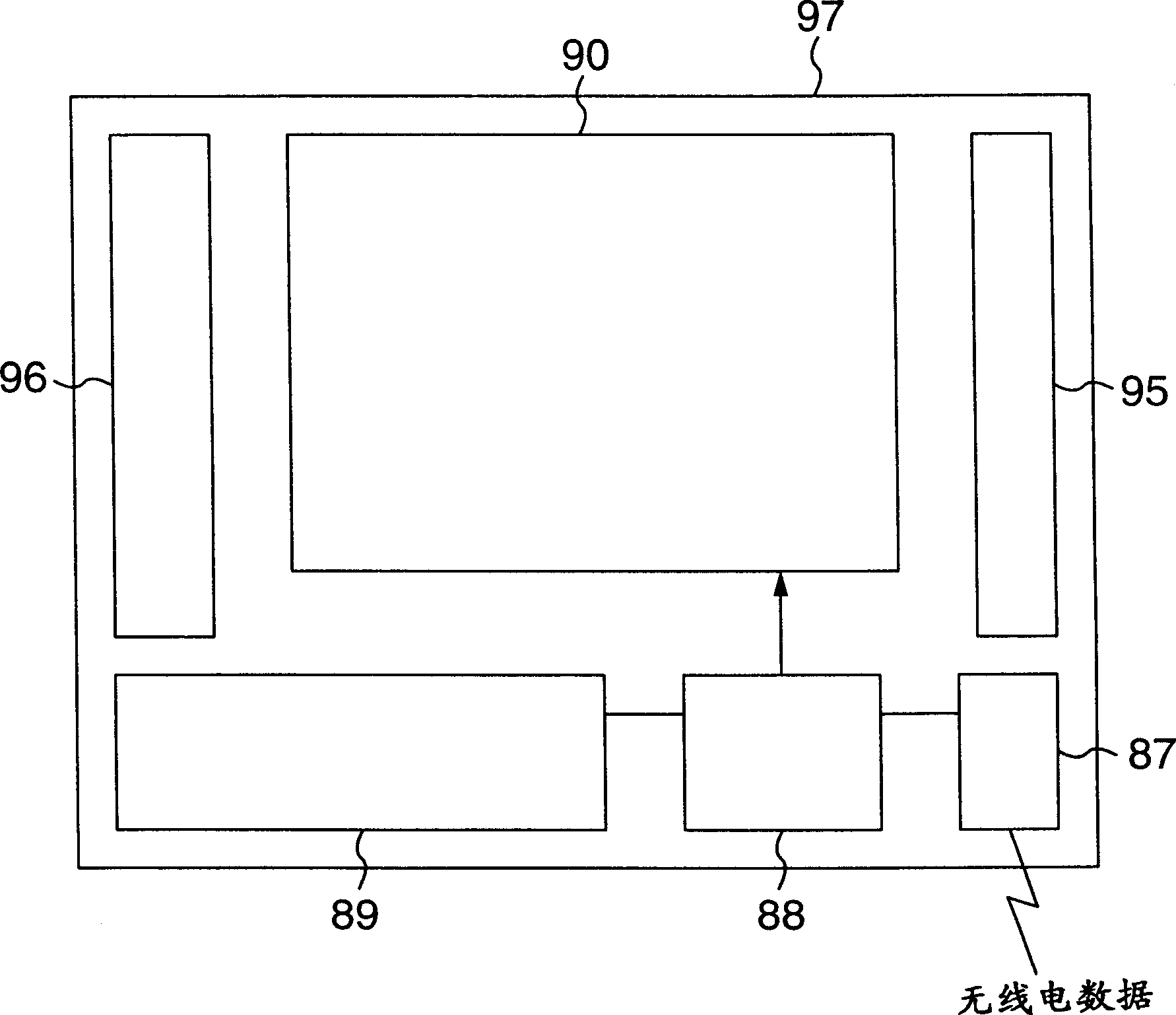
[0027] image 3 It is a block diagram of the image scope 97.

[0028] The image viewer 97 is composed of a radio interface (I / F) circuit 87, an MPU and decoder 88, a frame memory 89, a polycrystalline Si liquid crystal display panel 90, a power supply 95, and a light source 96. In the radio I / F circuit 87, the compressed image data is input as radio data from the outside according to the Bluetooth (bluetooth) specification, and the output signal of the radio I / F circuit 87 is stored in the frame memory through the MPU and decoder 88 89 in. The output signal of the MPU and decoder 88 is input to the polycrystalline Si liquid crystal display panel 90. The polycrystalline Si liquid crystal display panel 90 has the same structure as the liquid crystal display panel 250 described in the first embodiment.

[0029] Hereinafter, the operation of this embodiment will be described. The radio I / F circuit 87 takes in compressed image data from the outside, and transmits the data to the MPU and...

Embodiment 3

[0032] In the first and second embodiments, the liquid crystal capacitor 102 is used as the pixel 100 of the image display panel 250, and the Figure 4 In the third embodiment, it is characterized in that an organic light emitting diode (OLED, Organic Light Emitting Diode) is used as the pixel 300. Hereinafter, Example 3 will be described in detail.

[0033] The pixel 300 is composed of the following elements: a low-temperature poly-Si-TFT pixel switch 301 with a gate connected to the gate lead 103, a drain connected to the signal line 104, and a gate connected to the source of the pixel switch 301 The pixel driving TFT 302 of the extremely low-temperature polycrystalline Si-TFT is similarly connected to the holding capacitor 303 of the source of the pixel switch 301 and the organic light emitting diode 304 connected to the drain of the pixel driving TFT 302 in the forward direction. In addition, the source of the pixel driving TFT 302 and the other end of the holding capacitor 30...


PUM


Abstract

To attain the lowering of the cost of a picture display device by realizing entire circuits in a peripheral device with a general LSI having a low withstanding voltage equal to or lower than 5 V. In a picture display panel which has a pixel area (105) where pixels are arranged in a matrix shape, a gate line shift register (106), a DA converter (107), a latch circuit (108), a horizontal shift register (109) and a plurality of level shifting circuits (111) and which is made to be constituted on insulated substrates so that a signal from a picture signal data input terminal (125) is inputted to the panel, a high voltage generating circuit (212) consisting of capacitances and diodes is provided on the substrates and clocks which have amplitudes of a low voltage and have prescribed frequencies are inputted from the high voltage generating circuit input terminals (213), (214) to the circuit (212) and a constant voltage having a low voltage is inputted also from the constant voltage input terminal (215) to the circuit (212) and a high voltage is supplied from the output terminal (216) of the circuit (212) to respective level shifting circuits (111).

Description

Technical field [0001] The present invention particularly relates to an image display panel and an image scope of an image display device using liquid crystal or organic light emitting diodes, which can be manufactured at low cost. Background technique [0002] Below, use Figure 7 Explain the existing technology. [0003] Figure 7 It is a structural diagram of an image display panel 150 using a low-temperature polycrystalline Si-TFT liquid crystal, for example, in a conventional example. In the pixel region 105, the pixels 100 having the liquid crystal capacitor 102 and the pixel switch 101 composed of low-temperature polycrystalline Si-TFT are arranged in a matrix shape, and the gate of the pixel switch 101 is connected to the gate via a gate lead 103极lead shift register 106. In addition, the drain of the pixel switch 101 is connected to the DA converter 107 via the signal line 104, the output signal from the latch circuit 108 is input to the DA converter 107, and the output ...

Claims


Application Information

Patent Timeline
Patent Type & Authority Applications(China)
IPC IPC(8): G02F1/1368G02F1/133G09G3/20G09G3/30G09G3/32G09G3/36
CPCG09G2300/0842G09G3/3233G09G2330/02G09G2310/0289G09G3/3648G09G3/20
Inventor 秋元肇
Owner JAPAN DISPLAY INC
Why Eureka
Try Eureka