LPrinting head substrate, printing head, printing head box and its printer
A print head and substrate technology, applied in printing, automatic power control, electrical components, etc., can solve problems such as interference with high-speed data transmission
- Summary
- Abstract
- Description
- Claims
- Application Information
AI Technical Summary
Problems solved by technology
Method used
Image
Examples
no. 1 example
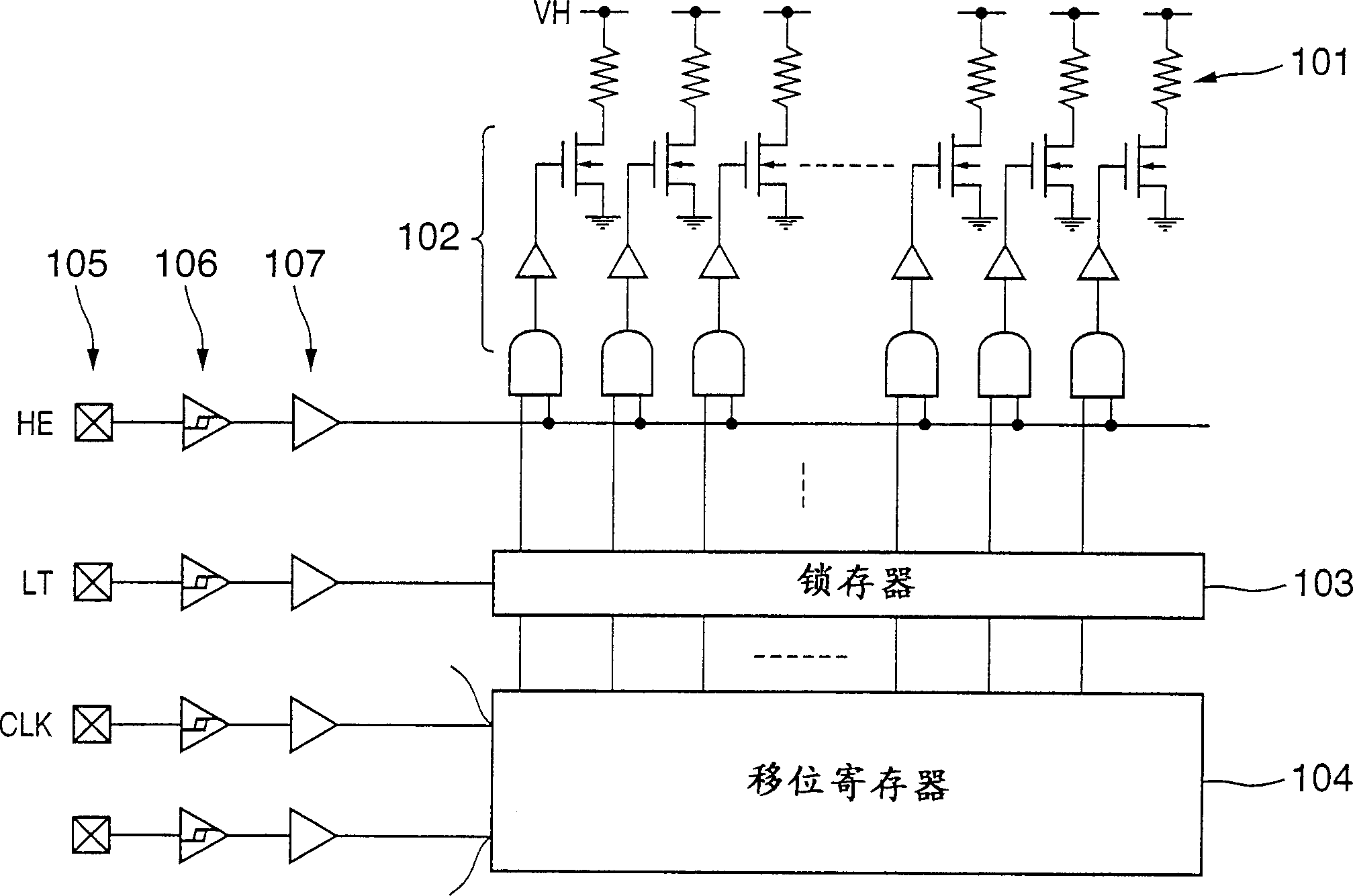
[0059] Figure 9 is a block diagram showing the construction of the print head chip according to the first embodiment of the present invention. for figure 2 Elements that are common to those shown in are denoted by the same reference numerals.
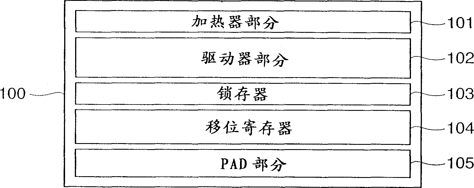
[0060] Each of the printhead dies 901 through 906 has a figure 1 The same circuit arrangement as the printhead die represented in . Assume that printing is performed by using six sheets of substrates 901 to 906 .
[0061] exist Figure 9 Among them, reference numeral 101 designates a heater portion (heater element) serving as an electrothermal transducer, reference numeral 102 designates a driver portion for driving each heater element according to print data, reference numeral 103 designates a latch circuit for latching print data, and reference numeral 103 designates a latch circuit for latching print data. 104 denotes a shift register that stores and holds a DATA signal serially input in synchronization with the CLK signal, an...
no. 2 example
[0068] Figure 10 is a circuit diagram showing the wiring of the DATA signal and the CLK signal on the print head chip according to the second embodiment of the present invention. for Figure 9 Elements common to those shown in are denoted by the same reference numerals, and descriptions thereof are omitted.
[0069] Figure 10 One capacitor 911 is shown connected to each output of buffer 107 for each DATA signal, as an example of time lag adjuster 910 . Here, it is assumed that the capacitance of each capacitor 911 is CL, and the input capacitances at the DATA input terminal and the CLK input terminal of each shift register 110 are CDATA and CCLK, respectively. It is further assumed that the on-resistances of the DATA signal and the CLK signal when driving the buffer circuit 107 are RDATA and RCLK, respectively, and that the number of shift registers 110 commonly connected to the CLK signal is n. Here, the time lag TDATA of the DATA signal input to each shift register 110...
no. 3 example
[0076] Figure 11 is a circuit diagram showing the wiring of the DATA signal and the CLK signal on the print head chip according to the third embodiment of the present invention. for Figure 9 and 10 Elements common to those shown in are denoted by the same reference numerals, and descriptions thereof are omitted.
[0077] Figure 11 One resistor 912 is shown connected to each output of buffer 107 for each DATA signal, as an example of time lag regulator 910 . Assuming that the resistance value of each resistor 912 is RL, the time lag TDATA of the DATA signal input to each shift register and the time lag TCLK of the CLK signal are described as follows:
[0078] TDATA≈(RDATA+RL)×CDATA
[0079] TCLK≈n×RCLK×CCLK
[0080] Here, the resistance value RL is set as follows:
[0081] RL=(n×RCLK×CCLK) / CDATA-RDATA
[0082] As a result, TDATA=TCLK holds true. With this, the difference between the time lag of the DATA signal input to each shift register 110 and the time lag of the...
PUM
 Abstract
Description
Claims
Application Information


