Printed circuit board with improved pad structure

A technology of printed circuit boards and pads, which is applied in the direction of printed circuits, printed circuits, printed circuit manufacturing, etc., and can solve the problems of lowering the overall level

Inactive Publication Date: 2003-02-12
SAMSUNG ELECTRONICS CO LTD
View PDF0 Cites 11 Cited by
  • Summary
  • Abstract
  • Description
  • Claims
  • Application Information

AI Technical Summary

Problems solved by technology

But this reduces the overall level of mounting peripheral chips on the printed circuit board 51

Method used


Image

  • Printed circuit board with improved pad structure
  • Printed circuit board with improved pad structure
  • Printed circuit board with improved pad structure

Examples


Embodiment Construction

[0019] Reference will now be made in detail to the detailed embodiments of the present invention in conjunction with the accompanying drawings, wherein like elements are numbered identically. The following embodiments are for explaining the present invention with reference to the figures.

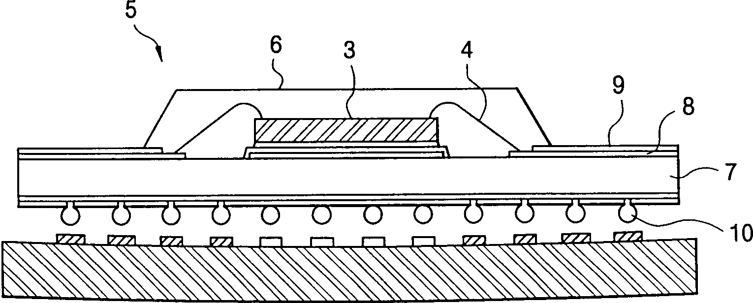
[0020] Such as figure 1 As shown, a BGA (ball grid array) package, as an example of a semiconductor chip package, is mounted on a printed circuit board according to the present invention, which is composed of a substrate 7 made of epoxy resin on A circuit pattern 8 formed on the substrate 7, a solder mask 9 coated on the circuit pattern 8, a semiconductor chip 3 mounted in the center of the substrate 7, and a wire 4 electrically connecting the circuit pattern 8 and the semiconductor chip 3. The semiconductor chip 3 and wires 4 are covered with a resin layer 6 to prevent oxidation and corrosion.

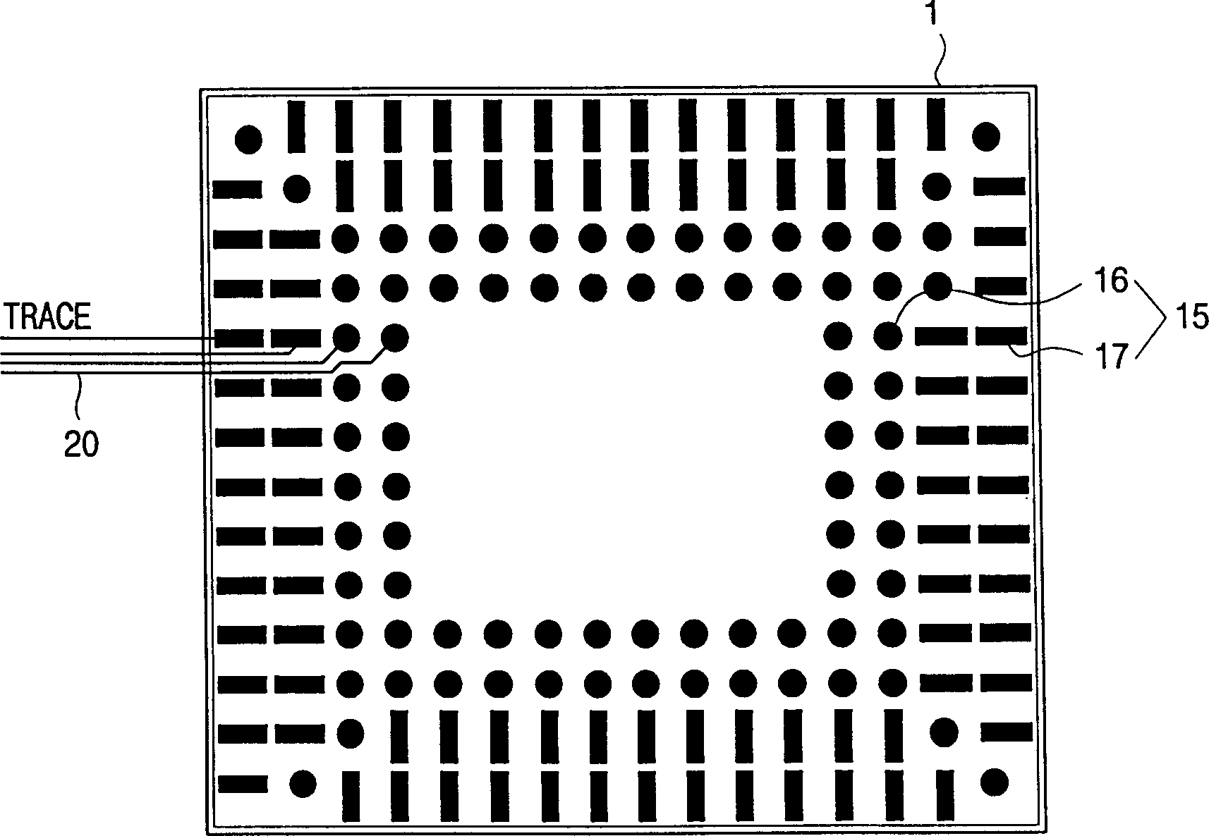
[0021] In the face of the printed circuit board 1 (refer to figure 2 ) has a plurality of s...


PUM


Abstract

A printed circuit board (PCB) having a plurality of lands corresponding to a plurality of solder pins provided on a semiconductor chip package, the lands provided adjacent to the border of the printed circuit board having a rectangular shape elongated in a direction toward the border, thus providing a printed circuit board which can achieve a simple design, improve the integration of peripheral chips mounted thereon, and secure a fine soldering state.

Description

field of invention [0001] The present invention relates generally to a printed circuit board (PCB), and more particularly to a printed circuit board with an improvement in the configuration of pads connected to solder balls of a semiconductor chip package. Background technique [0002] Generally, semiconductor chip packages are classified into dual in-line (DIP or IMT) type packages and surface mount (SMT) type packages. Recently, SMT packages are widely used to enhance package-to-PCB mounting efficiency on electrical equipment conforming to miniaturization, compared with IMT packages. As examples of the SMT package, there are QFP (Quad Flat Package), PLCC (Plastic Leaded Chip Carrier), CLCC (Ceramic Leaded Chip Carrier), BGA (Ball Grid Array), and the like. [0003] Such as figure 1 As shown, BGA package 5, as an example of SMT package, is composed of a substrate 7 made of ceramics or epoxy resin, a circuit pattern 8 formed on the substrate 7, and a circuit pattern coated...

Claims


Application Information

Patent Timeline
Patent Type & Authority Applications(China)
IPC IPC(8): H05K3/32H01L23/498H05K1/11H05K3/34
CPCH01L2924/15311H05K2201/09409H05K2201/09227H05K2201/094H05K2201/09418H01L24/48H01L23/49838H05K3/3436H05K2201/10734H01L2224/48227H05K1/111H01L2224/05599H01L2224/45099H01L2224/73265H01L2224/85399H01L2924/00014H01L2924/181Y02P70/50H01L2224/45015H01L2924/207H01L2924/00012H05K3/32
Inventor 郑成浩
Owner SAMSUNG ELECTRONICS CO LTD
Why Eureka
Try Eureka