Method for plating via hole with copper

A technology of via holes and copper plating, which is applied in circuits, printed circuits, printed circuits, etc., can solve the problem that the via holes cannot meet the thermal shock test.

Inactive Publication Date: 2003-03-12
TOYOTA IND CORP
View PDF0 Cites 11 Cited by
  • Summary
  • Abstract
  • Description
  • Claims
  • Application Information

AI Technical Summary

Problems solved by technology

If the filling and plating of the via hole is completed by simply increasing the current density in a short period of time, most of the via hole will not meet the requirements of the thermal shock test, which is one of the via hole reliability tests.

Method used


Image

  • Method for plating via hole with copper
  • Method for plating via hole with copper
  • Method for plating via hole with copper

Examples


Embodiment Construction

[0019] DETAILED DESCRIPTION OF THE PREFERRED EMBODIMENT

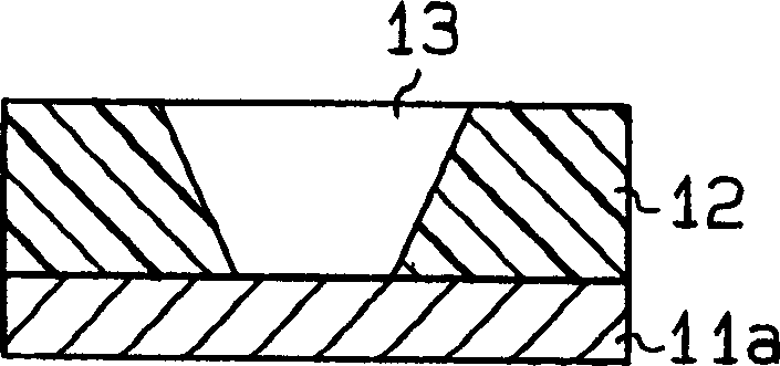
[0020] An embodiment of the method of forming a via hole of the present invention will be described below with reference to FIGS. 1(a) to 3(b). In this embodiment, the diameter of the formed via hole is 40 μm.

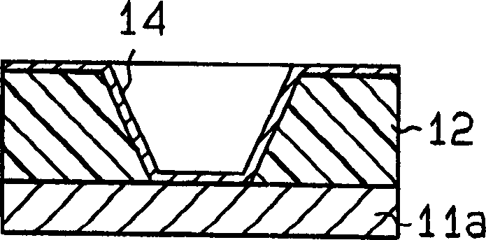
[0021] In order to form a conductive layer that fills the plated via hole to form an electrical connection on the upper and lower sides of the multilayer substrate, an insulating layer 12 is first formed on the bottom conductive layer 11a, and then, a via hole 13 is formed by laser radiation, As shown in Figure 1(a). Then carry out the degreasing method. A catalyst coating step and an electroless copper plating step are then performed on the inner wall of the via hole 13 and the upper layer forming the conductive layer 11b to form a thin electroless copper plating layer 14, as shown in FIG. 1(b).

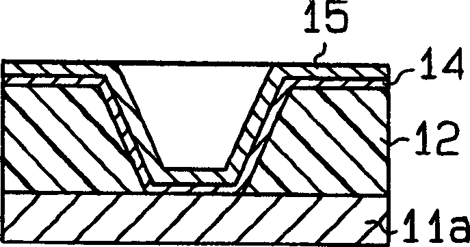
[0022] An electrolytic copper plating step is then performed. The electrolytic copper plati...


PUM

PropertyMeasurementUnit
thicknessaaaaaaaaaa
diameteraaaaaaaaaa
thicknessaaaaaaaaaa

Abstract

A copper plating method for a via hole formed on a multi-layer substrate is provided. The via hole interconnects conductive layers of the multi-layer substrate. The method includes performing chemical copper plating on an inner wall of the via hole and performing electrolytic copper plating on the inner wall of the via hole, on which the chemical copper plating has been performed. The electrolytic copper plating includes a first stage and second stage. The first stage is performed with a current density equal to or less than 1.5 A / dm2 to deposit copper film having a thickness of 1 mum or more. The second stage is performed at a current density higher than that in the first stage.

Description

field of invention [0001] The present invention relates to a copper plating method, and more particularly, the present invention relates to a method of copper plating a via hole for interconnecting wiring layers (conductor layers) in a multilayer substrate. Background of the invention [0002] Build-up wiring boards can be used to increase the density of multilayer wiring boards (multilayer substrates). Combo boards use via holes to connect wiring layers to each other. If the via hole is only used to connect two layers, the inner wall of the via hole does not need to be plated. However, when three or more layers are connected to each other, the via holes 31 not filled with plating metal must be replaced as shown in FIG. 4(a). On the other hand, via holes 31 filled with plating metal 32 can be stacked as shown in FIG. 4( b ), so that a high degree of freedom can be obtained in the arrangement of lines. [0003] Traditional vias are about 100 μm i...

Claims


Application Information

Patent Timeline
Patent Type & Authority Applications(China)
IPC IPC(8): H05K3/46H01L21/3205H05K3/42
CPCH05K2203/1476H05K2201/09563H05K3/421H05K2203/1492H05K3/423H01L21/3205
Inventor 下俊久井上敏树熊谷京子加藤祥文吉田贵司日高理仲
Owner TOYOTA IND CORP
Why Eureka
Try Eureka