Copper and copper bonding method

A copper-copper bonding and brazing technology, which is applied in the manufacture of electrical components, electrical solid devices, semiconductor/solid devices, etc., can solve the problems of poor bonding plasticity and the inability to realize the integration of dense pitches, and achieve simplified steps Effect

Inactive Publication Date: 2014-11-05
NAT CENT FOR ADVANCED PACKAGING
View PDF8 Cites 3 Cited by
  • Summary
  • Abstract
  • Description
  • Claims
  • Application Information

AI Technical Summary

Problems solved by technology

[0003] In the prior art, the patent WO 2012089105A1 discloses a spark plasma sintering process (SPS), the process temperature is between 200°C and 300°C, and the pressure is between 16 and 80MPa; but the bonding plasticity is poor, and the pitch cannot be achieved. intensive integration

Method used


Image

  • Copper and copper bonding method
  • Copper and copper bonding method
  • Copper and copper bonding method

Examples


Embodiment Construction

[0022] The present invention will be further described below in conjunction with specific drawings.

[0023] The copper-copper bonding method comprises the following process steps:

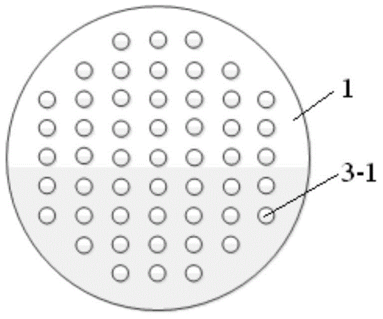
[0024] (1) if figure 1 As shown, the surface pretreatment of substrate 1 and chip 2 is carried out to make the surface of substrate 1 meet the process requirements. After pretreatment, the surface roughness is <0.3nm, there are no particles larger than 1 μm in size, and there is no organic residue on the surface. The copper solder joints on the substrate are 3 -1 The protrusion height is 100-500nm, and the surface flatness is less than 5%; the surface pretreatment method adopts: weak acid wet treatment (Formic Acid), plasma (plasma) treatment or chemical mechanical polishing (CMP);

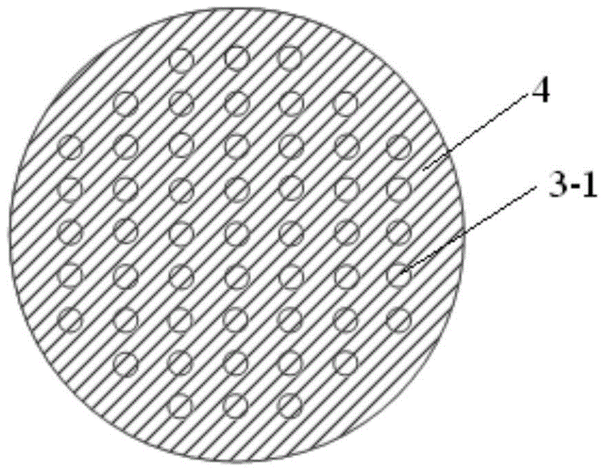
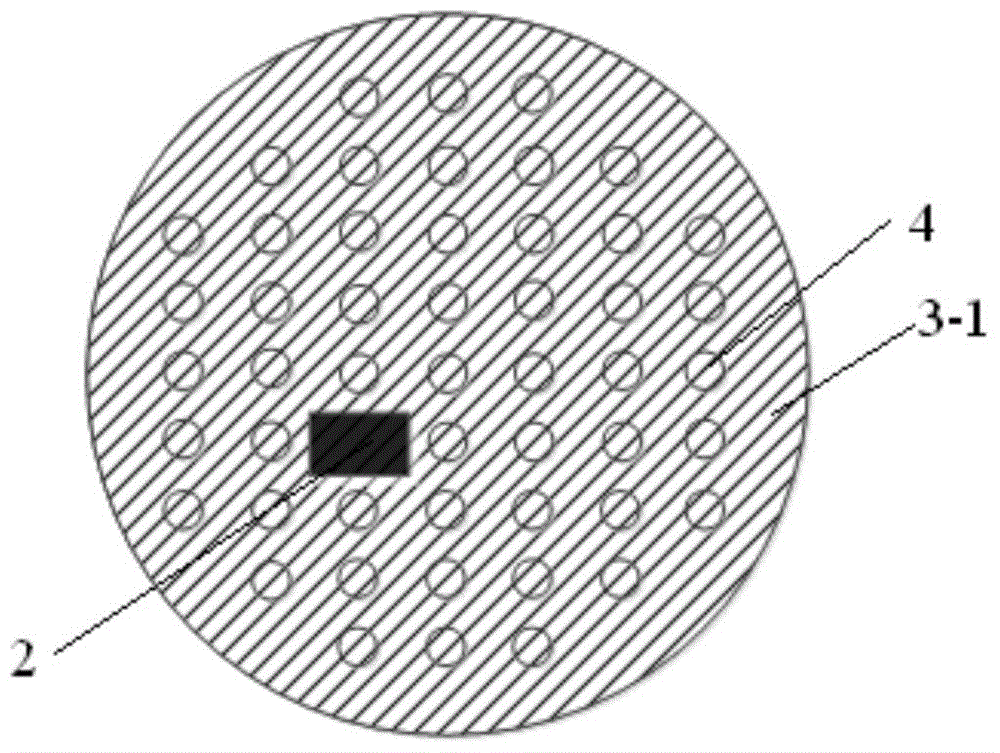
[0025] (2) if figure 2 As shown, a coating material 4 is covered by spin coating or vacuum lamination on the substrate 1, and the coating thickness is 1-5 μm, which is determined according to the process requiremen...


PUM


Abstract

The invention relates to a copper and copper bonding method. The copper and copper bonding method comprises the following technological steps that first, surface preprocessing is carried out on a substrate and a chip, so that the surface roughness of the substrate is smaller than 0.3nm, no particles with the diameter larger than 1 micron exist on the surface of the substrate, the protruding height of copper solder joints on the substrate ranges from 100 nm to 500 nm, and the surface evenness of the substrate is smaller than 5%; second, the substrate is covered with a layer of covering material in a spin coating mode or a vacuum lamination mode, wherein the covering material is epoxy resin or photodecomposition adhesive film or back-side adhesive film or thermoplastic resin or a light resistance material; third, copper solder spots of the chip are aligned with the copper solder spots of the substrate; fourth, the chip is fixed to the substrate through a soft pressing head in a closed space filled with inert gas, the temperature ranges from 150 DEG C to 250 DEG C, the pressure of the soft pressing head ranges from 50 kN to 100 kN, and the time ranges from 30 minutes to 3 hours; fifth, after curing is carried out, a plurality of chips are stacked on the chip according to the steps. According to the copper and copper bonding method, high-density integration of copper wires super-dense pitches can be achieved, and fixation carried out after bonding is completed at the temperature lower than 200 DEG C.

Description

technical field [0001] The invention relates to a copper-copper bonding method, which belongs to the technical field of semiconductor packaging. Background technique [0002] With the vigorous development of the microelectronics industry, the integrated circuit electronic packaging industry is rapidly advancing towards the direction of small size, high performance, high density, and multi-chip. Therefore, the ultra-fine pitch of copper leads (such as 3 μm, 6 μm ) makes more sense. [0003] In the prior art, the patent WO 2012089105A1 discloses a spark plasma sintering process (SPS), the process temperature is between 200°C and 300°C, and the pressure is between 16 and 80MPa; but the bonding plasticity is poor, and the pitch cannot be achieved. Dense integration. Patent US 20080315421A1 discloses a surface-active bonding (SAB), which is carried out at room temperature and uses ultra-high vacuum pressure to bond the surface, but has higher requirements for surface cleanlines...

Claims


Application Information

Patent Timeline
Patent Type & Authority Applications(China)
IPC IPC(8): H01L21/603
CPCH01L24/81H01L2224/80001
Inventor 林挺宇顾海洋李婷
Owner NAT CENT FOR ADVANCED PACKAGING
Why Eureka
Try Eureka