Integrated radio-frequency circuit

A circuit and amplifying circuit technology, applied in the field of radio frequency equipment and wireless network equipment, can solve the problems of logic circuit noise, adverse effects of the operation of on-chip radio frequency components, etc.

Inactive Publication Date: 2003-03-19
ALTERA CORP
View PDF6 Cites 1 Cited by
  • Summary
  • Abstract
  • Description
  • Claims
  • Application Information

AI Technical Summary

Problems solved by technology

Logic circuits can generate noise that can adversely affect the operation of on-chip RF components du

Method used


Image

  • Integrated radio-frequency circuit
  • Integrated radio-frequency circuit
  • Integrated radio-frequency circuit

Examples


Embodiment Construction

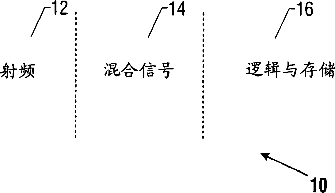
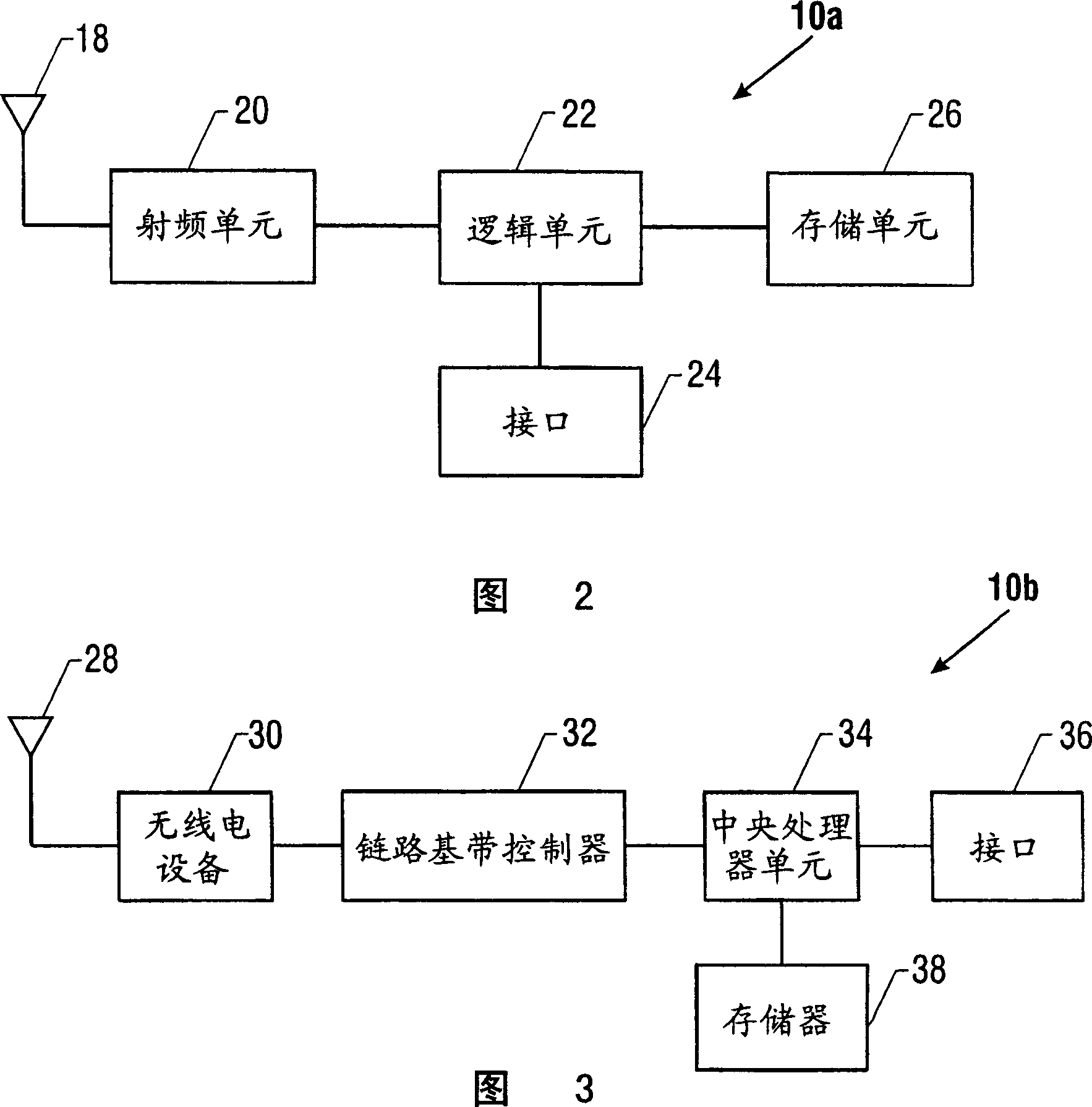
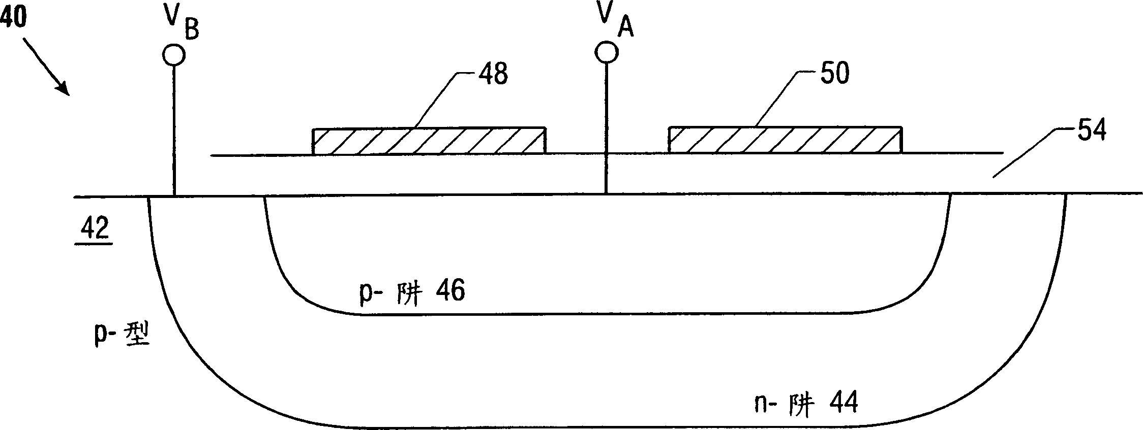
[0034] refer to figure 1 , integrated circuit 10 may include analog circuit elements operating above 100 MHz, such as radio frequency elements 12, mixed signal elements 14, and logic and memory elements 16, all integrated within the same monolithic integrated circuit. Coupling between RF circuit components (such as inductors, capacitors, and transistors) and the substrate, if not effectively eliminated, can be reduced by creating effective reverse-biased diodes between the RF components and the substrate. Such reverse-biased diodes can be formed using a triple well fabrication process in which inductive circuit elements and transistors are formed on separate triple wells.

[0035] In addition, storage elements such as flash memory and static random access memory (SRAM) can be fabricated on the same substrate using the same methods that form logic circuits such as microprocessors and digital signal processors. For example, the methods disclosed in US Patent Nos. 5,926,418 and ...


PUM


Abstract

An RF circuit (310) may be formed over a triple well (316, 318, 320) that creates two reverse biased junctions. By adjusting the bias across the junctions, the capacitance across the junctions can be reduced, reducing the capacitive coupling from the RF circuits (310) to the substrate (316), improving the self-resonance frequency of inductors and reducing the coupling of unwanted signals and noise from the underlying substrate to the active circuits and passive components such as the capacitors and inductors. As a result, radio frequency devices, such as radios, cellular telephones and transceivers such as Bluetooth transceivers, logic devices and Flash and SRAM memory devices may all be formed in the same integrated circuit die using CMOS fabrication processes.

Description

technical field [0001] The present invention relates generally to radio frequency (RF) integrated circuits including active devices and passive components such as inductors and personal digital assistant). Background technique [0002] By convention, integrated circuits are divided into different categories in the integrated circuit manufacturing process depending on the compatibility of the process and other considerations. Generally speaking, RF circuits should not be mixed with logic circuits in the same integrated circuit. Radio frequency circuits are analog circuits involved in the filtering and detection of radio frequency signals, such as cellular telephone signals. In contrast, logic circuits generally contain transistors and other active elements that make up integrated circuit devices. For example, bipolar technology can be used to make radio-frequency circuits, while standard complementary metal-oxide-semiconductor (CMOS) processes can be used to make logic cir...

Claims


Application Information

Patent Timeline
IPC IPC(8): H01L21/822H01L21/02H01L21/761H01L21/8234H01L21/8238H01L23/522H01L27/04H01L27/06H01L27/08H01L27/088H01L27/092
CPCH01L2924/0002H01L27/0928H01L27/088H01L27/08H01L21/823481H01L2924/3011H01L28/10H01L23/5227H01L21/761H01L2924/00
Inventor 王鼎华C·L·胡
Owner ALTERA CORP
Why Eureka
Try Eureka