Output circuit

A technology for outputting circuits and outputting power, which is applied in logic circuit connection/interface layout, electronic switches, electrical components, etc., and can solve problems such as inability to operate semiconductor storage devices at high speed, reduction of current drive capability, and acceleration

Inactive Publication Date: 2003-04-30
MITSUBISHI ELECTRIC CORP
View PDF0 Cites 7 Cited by
  • Summary
  • Abstract
  • Description
  • Claims
  • Application Information

AI Technical Summary

Problems solved by technology

Therefore, if the H level of the internal signal INN applied to the gate of the N-channel MOS transistor NQ is at the output power supply voltage VDDQ level, the current drive capability of the N-channel MOS transistor NQ is also reduced, and the output node cannot be supplied at high speed. discharge
[0013] This lowering of the output power supply voltage is evident in semiconductor memory devices. When the operating speed of the output circuit is reduced at a low power supply voltage, the operating speed of the semiconductor memory device is accelerated according to the law of the operating speed of the output circuit, and it cannot be operated at high speed. A semiconductor memory device cannot construct a system that performs high-speed processing at a low power supply voltage

Method used


Image

  • Output circuit
  • Output circuit
  • Output circuit

Examples


Embodiment 1

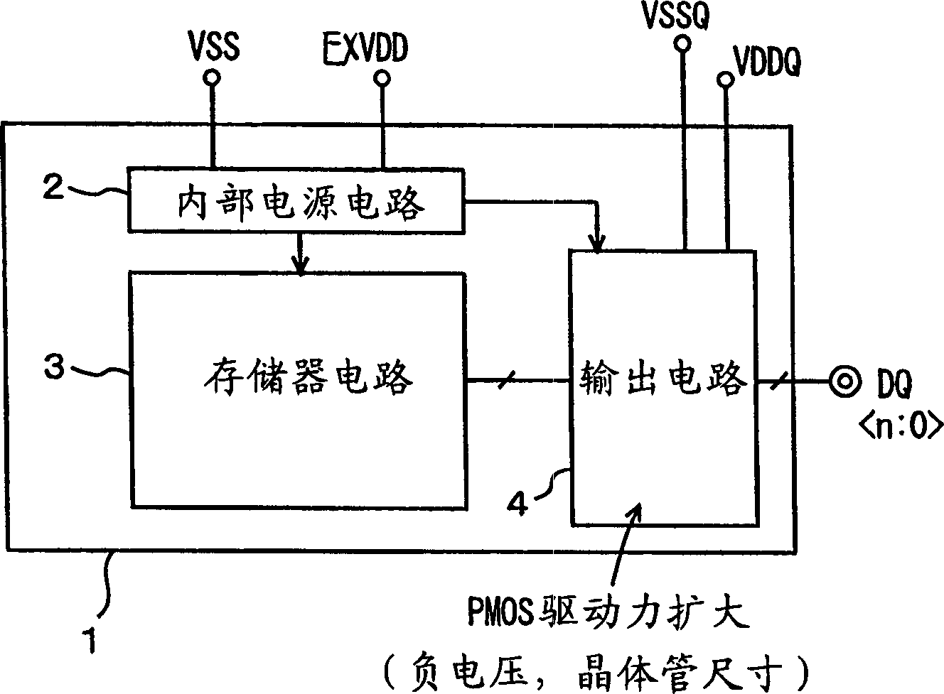
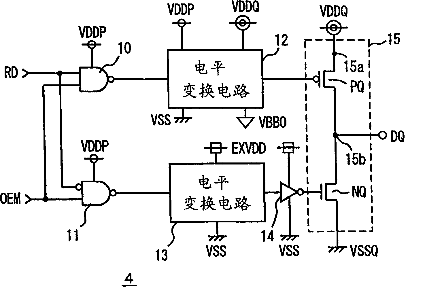
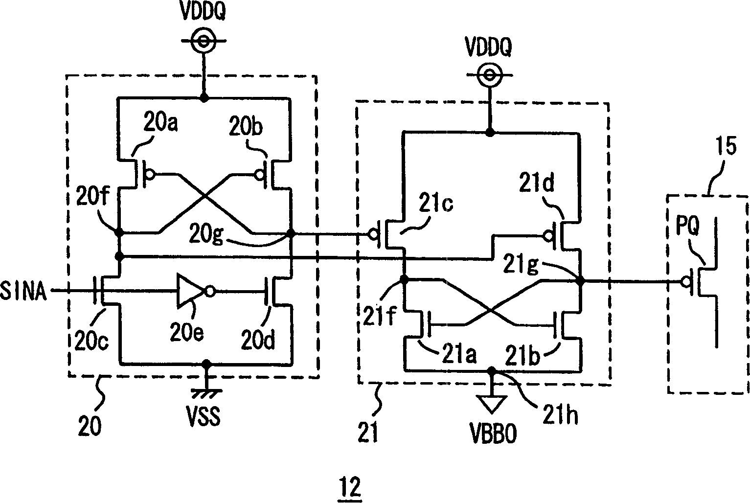
[0059] figure 2 is a diagram schematically showing the configuration of the output circuit 4 according to Embodiment 1 of the present invention. figure 2 Among them, the output circuit 4 includes a NAND circuit 10 that receives the internal read data RD read from the memory circuit 3 and the output permission signal OEM from the output control circuit included in the memory circuit 3, receives the internal read data RD and the output permission signal The gate circuit 11 of the OEM, the level conversion circuit 12 that converts the output signal of the NAND circuit 10 into a signal varying between the output power supply voltage VDDQ and the negative voltage VBB0, and converts the output signal of the gate circuit 11 into an output signal at the external power supply voltage EXVDD A level conversion circuit 13 for signals varying between ground voltage VSS, an inverter 14 receiving the output signal of the level conversion circuit 13, and a device for generating output data ...

Embodiment 2

[0088] Figure 5 is a diagram schematically showing the configuration of an output circuit according to Embodiment 2 of the present invention. Figure 5 In, the circuit portion for driving the pull-down N-channel MOS transistor NQ of the output buffer circuit 15 is the same as figure 2 The structures shown are the same, and the corresponding parts are given the same reference numbers, and the detailed description thereof is omitted.

[0089] Should Figure 5 In the output circuit 4 shown, in order to drive the gate of the pull-up P-channel MOS transistor PQ included in the output buffer circuit 15 to a negative voltage level, a charge pump operation using a capacitor is performed (capacitive coupling).

[0090] which is, Figure 5 Among them, the output circuit 4 includes a level conversion circuit 30 for converting the amplitude of the output signal of the NAND circuit 10 into an output power supply voltage VDDQ level, an inverter 31 for inverting the output signal of the...

Embodiment 3

[0110] Figure 7 is a diagram schematically showing the configuration of an output circuit according to Embodiment 3 of the present invention. Figure 7 In the output circuit 4, the structure of the circuit part that drives the N-channel MOS transistor NQ included in the output buffer circuit 5 is the same as figure 2 The structures of the output circuits shown are the same, and the corresponding parts are given the same reference numbers, and the detailed description thereof is omitted.

[0111] Should Figure 7 In the output circuit 4 shown, a capacitive element 41 is provided between the gate of the pull-up P-channel MOS transistor PQ of the output buffer circuit 5 and the output of the NAND circuit 10 . In order to realize the charge pump operation of the capacitive element 41, the output circuit 4 further includes a level conversion circuit 40 that converts the amplitude of the output signal of the NAND circuit 10 into the amplitude of the output power supply voltage V...


PUM


Abstract

The invention drives output nodes with optimum drive capability even when the voltage of the output line voltage is changed. The output circuit (4) changes the transistor size or the negative voltage according to the output power supply voltage (VDDQ) to adjust the drive capability of its output transistor. Especially, even when the output power supply voltage is made to be lower by expanding the drive capability of a P-channel MOS transistor, it is possible to generate output output signals at high speed by suppressing the lowering of the driving power.

Description

technical field [0001] The present invention relates to an output circuit, in particular to an output circuit structure capable of outputting signals at a high speed even at a low power supply voltage. Background technique [0002] Figure 24 It shows an example of the configuration of the final output stage of a conventional output circuit. Figure 24 , the output circuit includes a P-channel MOS transistor (insulated gate field effect transistor) PQ connected between the power supply node and the output node ON and receiving the internal signal INP at its gate and connected between the output node ON and the ground point And an N-channel MOS transistor NQ receiving an internal signal INN at its gate. An output signal DQ is output to the output node ON. [0003] The internal signals INP and INN are signals of the same logic level generated by an output drive control circuit not shown. [0004] When the internal signals INP and INN are both at the H level, the MOS transist...

Claims


Application Information

Patent Timeline
Patent Type & Authority Applications(China)
IPC IPC(8): G11C11/417G06F3/00G11C7/10G11C11/40G11C11/413H03K17/04H03K17/687H03K19/0175
CPCG11C7/1057G11C7/1051G11C11/40
Inventor 冈本武郎山内忠昭松本淳子石田耕三米谷英树长泽勉
Owner MITSUBISHI ELECTRIC CORP
Why Eureka
Try Eureka