Structure and method for packaging colour light-emitting diode with stacked wafer

A technology of light-emitting diodes and packaging structures, which is applied to electrical components, circuits, semiconductor devices, etc., and can solve problems such as difficult heat dissipation, shortened life, and difficult and precise control

Inactive Publication Date: 2003-06-11
张修恒
View PDF0 Cites 33 Cited by
  • Summary
  • Abstract
  • Description
  • Claims
  • Application Information

AI Technical Summary

Problems solved by technology

The package structure of the above-known full-color LED is completely supplied with 20mA current, and the method of combining various colors with different lighting time lengths is very difficult to control accurately, and the design of the power control IC is also very complicated.
And the current is fixed, the heat is lar...

Method used


Image

  • Structure and method for packaging colour light-emitting diode with stacked wafer
  • Structure and method for packaging colour light-emitting diode with stacked wafer
  • Structure and method for packaging colour light-emitting diode with stacked wafer

Examples


Embodiment Construction

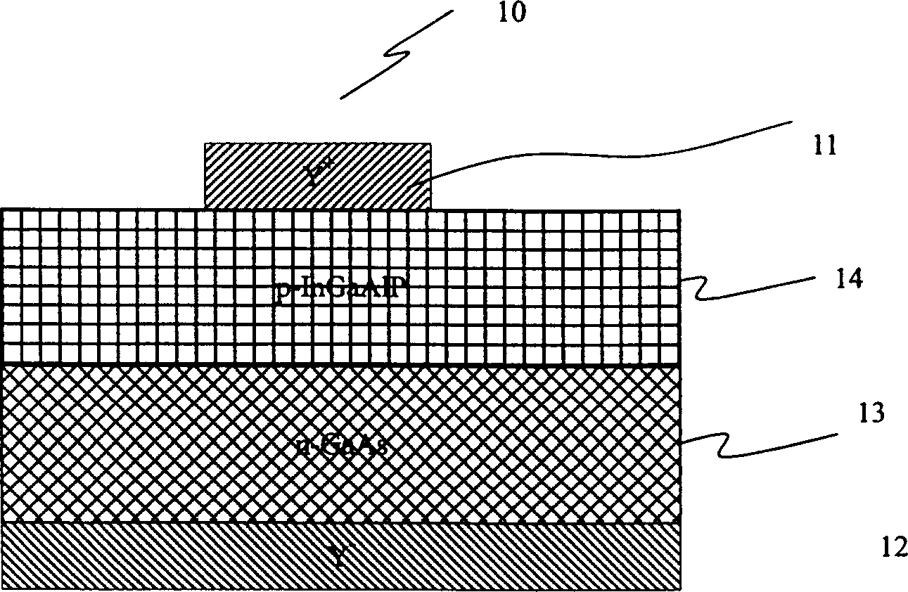
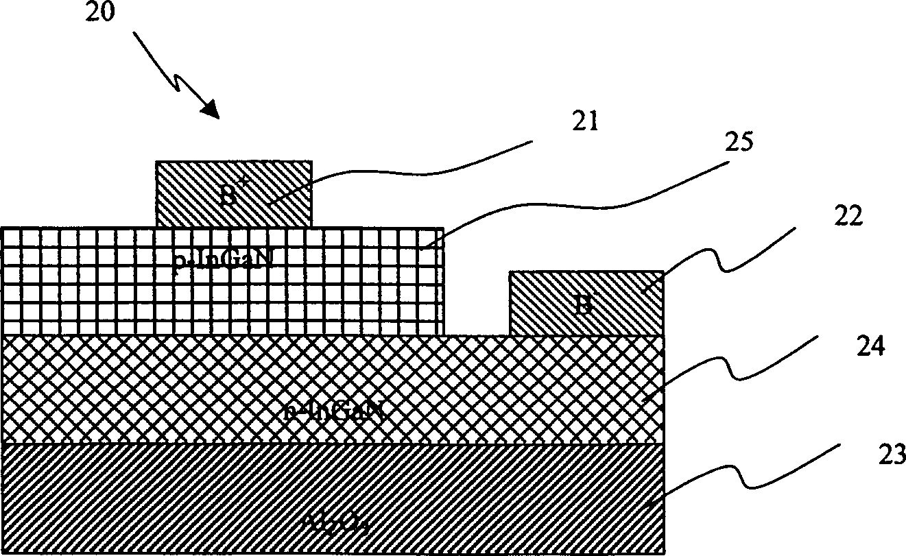
[0065] The content of the present invention can be illustrated by the following embodiments and the accompanying drawings. The various LED materials used in the present invention are not limited, as long as they are LED chips capable of emitting three primary colors of red, green, blue and yellow. The wafer can be produced by a known method, and can be manufactured according to the specifications (size, bias value, brightness, color, metal contact material, etc.) specified in the present invention. Structures according to the present invention should be measured and graded prior to encapsulation, using the same grade or the same type (eg, bias, brightness, color) for the same encapsulation.

[0066] The invention includes a printed circuit board with a pattern of a metal reflective layer on it for die bonding. After the first chip is bonded, the second chip is stacked on the first chip for die bonding. The method can be thermal fusion, ultrasonic fusion or bonding with transp...


PUM

PropertyMeasurementUnit
Thicknessaaaaaaaaaa
Thicknessaaaaaaaaaa
Thicknessaaaaaaaaaa

Abstract

This invention discloses a laminated chip full color LED package structure and method mainly utilizing the package technology to die bond more than two various single-colour LED by lamination by heat or supersonic wave with metal oxide transparent conductive layer and metal reflection layer to make the lower layer of monocolour light mix with another via the transparent conductive layer to generate another color light source. The lowest is die bonded with metal reflection layer to reflect different colors of light and increase its intensity. In near distance, white or full color light are displayed and a full color LED is got by laminating the three basic colors while for remote two separated LED are used eg. yellow blue or red, green.

Description

technical field [0001] The invention relates to a packaging structure and method for full-color light-emitting diodes, in particular to an LED that stacks chips to mix monochromatic light into a color light source to provide full-color display. Background technique [0002] Light Emitted Diode (LED) is a device made of semiconductor materials and a very small solid-state light source that converts electrical energy into light. Not only is it small in size, but also has a long life, low driving voltage, fast response rate, and good shock resistance. It can meet the needs of light, thin and miniaturized equipment for various applications, and has already become a very popular product in daily life. [0003] Light-emitting diodes are LEDs with various colors such as red, orange, yellow, green, blue, and violet, as well as invisible light such as infrared and ultraviolet, using various compound semiconductor materials and changes in device structure. Materials suitable for maki...

Claims


Application Information

Patent Timeline
IPC IPC(8): H01L33/00
Inventor 张修恒
Owner 张修恒
Why Eureka
Try Eureka