Circuit board device and its mounting method

A technology of circuit boards and printed circuit boards, applied in the direction of circuits, printed circuits, printed circuits, etc., can solve the problems of unable to absorb the warping of printed circuit boards, unstable connection status, poor connection of bosses, etc.

Inactive Publication Date: 2003-06-25
MURATA MFG CO LTD
View PDF1 Cites 5 Cited by
  • Summary
  • Abstract
  • Description
  • Claims
  • Application Information

AI Technical Summary

Problems solved by technology

[0009] However, if a large boss is formed, the solder that should protrude toward the mother board side will spread and become thinner along the boss during the solder mounting operation, so as long as a large amount of solder does not adhere to the boss, it will cause soldering. Insufficient protrusion size, unable to absorb warping of the printed circuit board, and prone to poor connection of bosses
[0010] In view of this point, when a large amount of solder is attached to the boss, not only the consumption of solder will increase uselessly, but also when the printed circuit board is mounted, the solder that melts and spreads between the boss and the mother board will sometimes cause adjacent There is a short circuit between the bosses, so there is a limit to increasing the amount of solder attached
[0011] Therefore, in the prior art, since it is difficult to obtain a suitable size for the boss area and the protruding size of the solder at the same time, it is impossible to mount the printed circuit board on the motherboard with sufficient strength, or the connection state of each boss, etc. become unstable, or become less reliable

Method used


Image

  • Circuit board device and its mounting method
  • Circuit board device and its mounting method
  • Circuit board device and its mounting method

Examples


Embodiment 2

[0096] then, Figure 10 Embodiment 2 of the present invention was shown, and this embodiment is characterized in that a partition wall is constituted by a mesh member. It should be noted that, in this embodiment, the same symbols are used for the same components as in the first embodiment, and their descriptions are omitted.

[0097] 21 is a partition wall provided on the back surface 1B side of the module printed circuit board 1, and this partition wall 21 divides the metal film 5 into a main boss 8 and an auxiliary boss 9 almost as in the embodiment. However, the partition wall 21 is not a part of the protective layer film 6', but is formed by printing a screen member such as ink or paint on the metal film 5, for example, by screen printing or the like.

[0098] Therefore, also in the embodiment having such a structure, almost the same effect as that of the first embodiment can be obtained. Furthermore, particularly in the present embodiment, the partition wall 21 can be e...

Embodiment 3

[0099] then, Figure 11 Embodiment 3 of the present invention is shown, and this embodiment is characterized in that the main lands and the auxiliary lands are formed by separate metal films, and the gaps between the respective metal films constitute partition walls. It should be noted that, in this embodiment, the same symbols are used for the same components as in the first embodiment, and their descriptions are omitted.

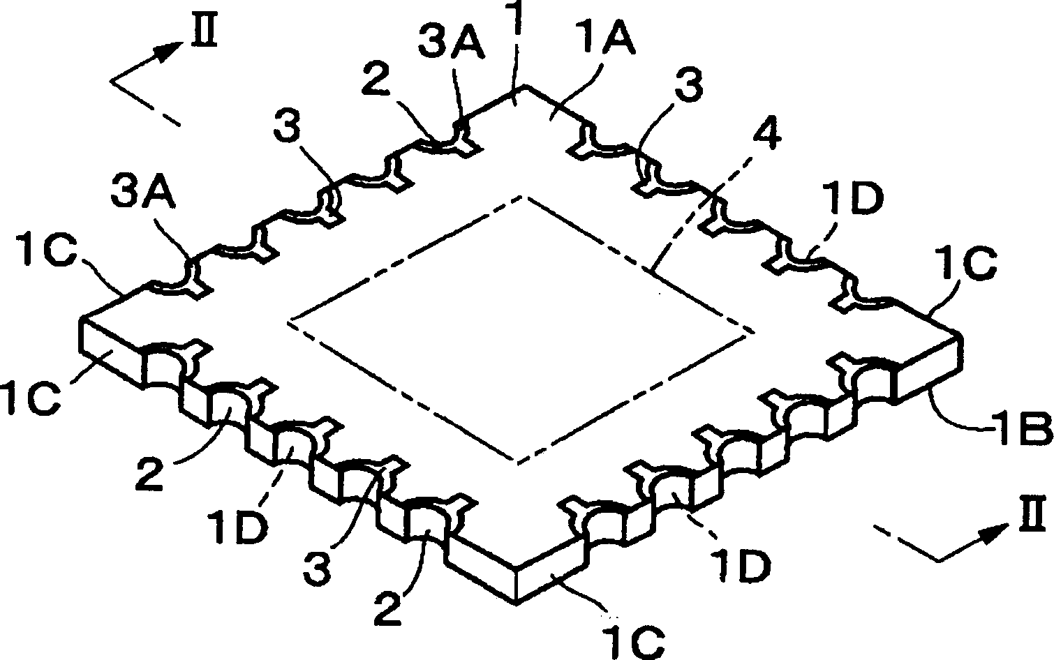
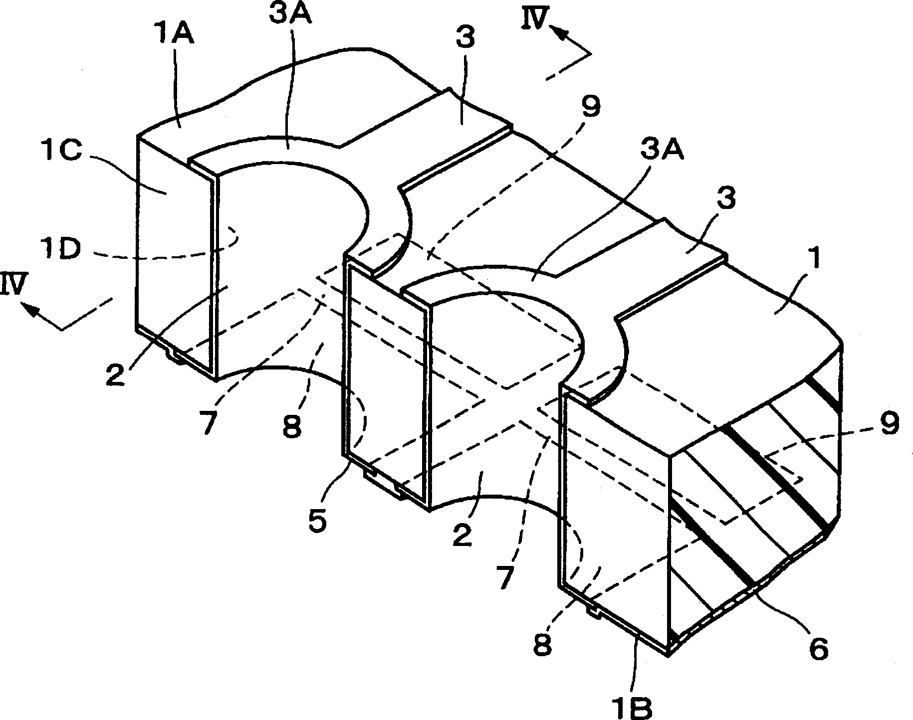
[0100] 3 1 is the main boss provided on the back side 1B of the module printed circuit board 1, the main boss 3 is almost the same as the embodiment 1, for example, it is formed of a nearly quadrangular metal film or the like, and is outside the printed circuit board 1. The edge side is connected to the end face electrode 2.

[0101] 32 is an auxiliary boss 32 that is provided on the back side 1B of the module printed circuit board 1 using a metal film or the like provided separately from the main boss 31. The inner sides of the printed circuit board 1 a...

Embodiment 4

[0104] then, Figure 12 Embodiment 4 of the present invention is shown, and this embodiment is characterized in that the main boss is formed in a substantially circular structure having an area larger than that of a semicircular shape. It should be noted that, in this embodiment, the same symbols are used for the same components as in the first embodiment, and their descriptions are omitted.

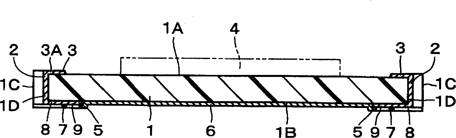
[0105]41 is a square metal film provided on the back surface 1B of the module printed circuit board 1 , and this metal film 41 is connected to the end surface electrodes 2 at positions surrounding the respective grooves 1D of the printed circuit board 1 almost as in the first embodiment.

[0106] 42 is a protective layer film provided on the back surface 1B side of the module printed wiring board 1, and the protective layer film 42 covers the back surface 1B side of the printed wiring board 1 including the peripheral portion of the metal film 41 and the like. In addition, the protective...


PUM


Abstract

In a circuit board, when lands provided on a rear surface of a substrate are each separated into a mainland and a sub-land, warping or other defects of the substrate can be ignored when soldering, and the substrate can be mounted with a high bonding strength. On the rear surface of a module substrate, partitions are each provided to separate a metal film into the mainland and the sub-land. Accordingly, when the substrate is mounted on a motherboard, solder applied beforehand from each end-surface electrode to the mainland can be largely protruded downward from the mainland, and warping or other defects of the substrate can be ignored by this protruding portion of the solder. In addition, in the state in which the substrate is mounted, since the solder is pushed out from between the mainland and the motherboard and overflows the partition, both the mainland and the sub-land can be soldered to the motherboard side, and hence stable bonding can be obtained at a large bonding area.

Description

technical field [0001] The present invention relates to a circuit board device and its mounting method for partially assembling electronic parts to be suitable for mounting on a mother board. Background technique [0002] Generally, as a circuit board device, for example, there is a structure in which a plurality of electronic components are partially assembled on a module printed circuit board (for example, refer to Patent Document 1). [0003] [Patent Document 1] JP-A-2001-127188 [0004] This circuit board device based on the prior art is composed of the following parts: a printed circuit board with electronic parts mounted on the front side and mounted on the motherboard on the back side; And connected to a plurality of end-face electrodes of electronic parts; connected to the end-face electrodes, and arranged on the back side of the printed circuit board, and soldered together with the end-face electrodes to a plurality of bosses on one side of the motherboard (land)....

Claims


Application Information

Patent Timeline
Patent Type & Authority Applications(China)
IPC IPC(8): H05K1/11H01L23/12H05K1/18H05K3/34H05K3/36
CPCH05K3/3442H05K2201/09663H05K3/368H05K2201/099H05K2201/09381Y10T29/49149H05K2201/09181Y10T29/49144Y10T29/49126H05K2201/10984H05K3/3452Y02P70/50H01L23/12
Inventor 福边建次冈田雅信中谷和义
Owner MURATA MFG CO LTD
Why Eureka
Try Eureka