

Semiconductor memory with read amplifier
A sense amplifier and memory technology, applied in the direction of static memory, digital memory information, information storage, etc.
- Summary
- Abstract
- Description
- Claims
- Application Information
AI Technical Summary
Problems solved by technology
Method used
Image

Examples
Embodiment 1
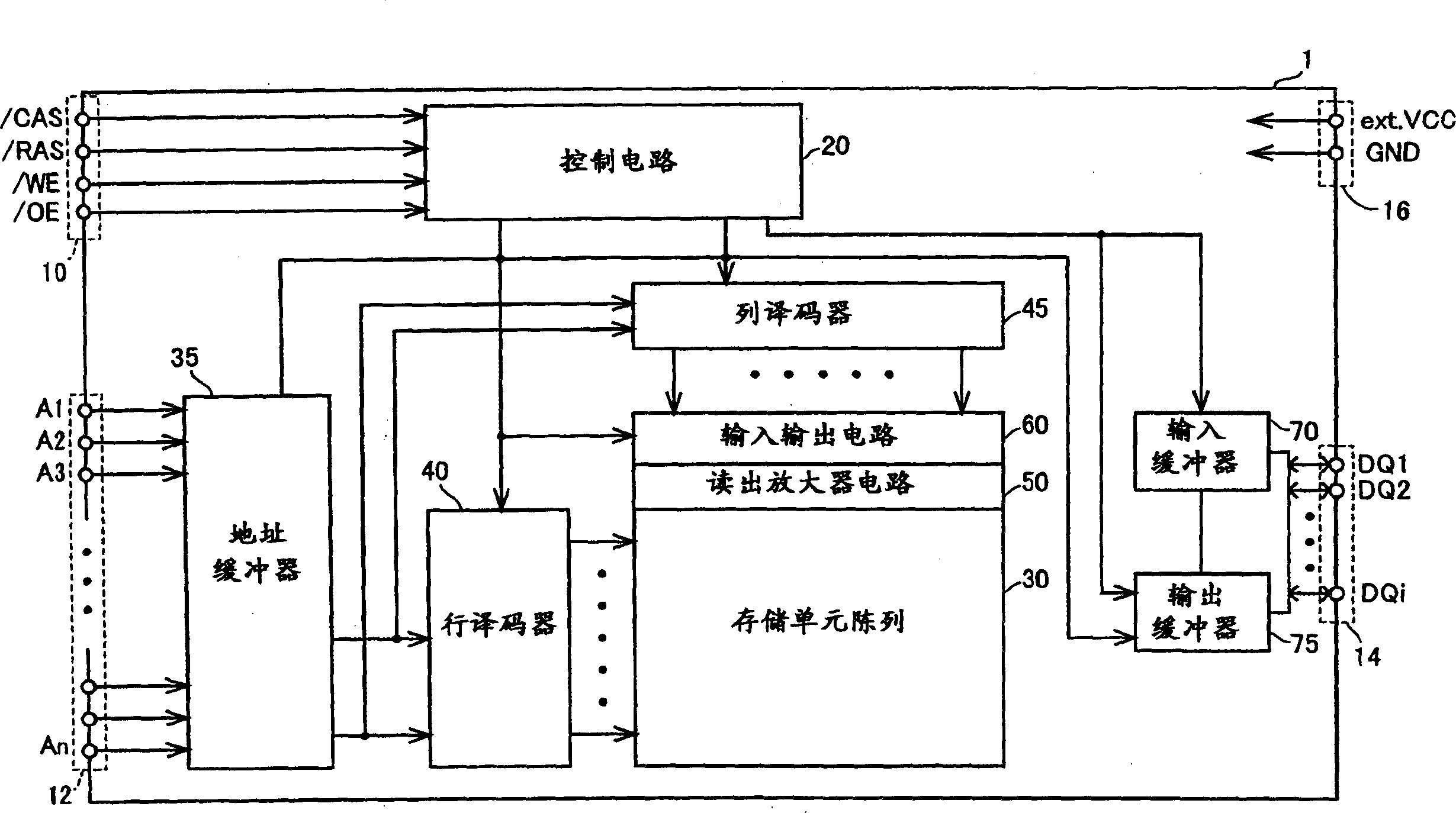
[0096] figure 1 It is a schematic block diagram showing the overall structure of the semiconductor memory in the embodiment of the present invention.
[0097] refer to figure 1 , the semiconductor integrated circuit device 1 includes: a control signal input terminal 10, which accepts the following control signals, namely column address strobe signal / CAS or row address strobe signal / RAS or write enable signal / WE or output enable signal / OE; Address input terminal 12 receives address signals A1 to An (n: natural number); and input terminal 14 receives and receives input and output data DQ1 to DQi (i: natural number).
[0098] The semiconductor integrated circuit device 1 further includes: a control circuit 20; a memory cell array 30; an address buffer 35; a row decoder 40 and a column decoder 45; a sense amplifier circuit 50; an input-output circuit 60; an input buffer 70; and an output buffer 75 .
[0099] The control circuit 20 controls the overall operation of the semic...
Embodiment 2
[0144] Figure 7 It is a circuit diagram showing the configuration of a sense amplifier and its peripheral circuits in the semiconductor memory in Embodiment 2 of the present invention.
[0145] refer to Figure 7 ,and Figure 4 In contrast, in the semiconductor memory of Embodiment 2, an equalizer 153 is provided instead of the equalizer 151 , and an equalizer 154 is provided instead of the equalizer 152 .
[0146] In the equalizer 153, compared with the equalizer 151, the transistor QN23 for equalization is omitted. In the equalizer 154, compared with the equalizer 152, the transistor QN43 for equalization is removed.
[0147] Since the other circuit configurations are the same as those of the first embodiment, the description thereof will not be repeated.
[0148] The read operation of the semiconductor memory having the above circuit configuration will now be described.
[0149] In addition, the read operation of the semiconductor memory of the second embodiment will ...
Embodiment 3
[0161] Figure 10 It is a circuit diagram showing the configuration of a sense amplifier and its peripheral circuits in the semiconductor memory in Embodiment 3 of the present invention.
[0162] refer to Figure 10 ,and Figure 7 In contrast, in the semiconductor memory device of Embodiment 3, an equalizer 155 is provided instead of the equalizer 153 , and an equalizer 156 is provided instead of the equalizer 154 .
[0163] In the equalizer 155, compared with the equalizer 153, the signal input to the gate of the transistor QN21 is the selection signal SEL2 instead of the precharge signal P1. In addition, the signal input to the gate of the transistor QN22 is the selection signal SEL1 instead of the precharge signal P2.
[0164] Similarly, in the equalizer 156, compared with the equalizer 154, the signal input to the gate of the transistor QN41 is the selection signal SER2 instead of the precharge signal P3. In addition, the signal input to the gate of the transistor QN42...
PUM
 Abstract
Description
Claims
Application Information