Acoustic surface wave device

A surface acoustic wave and end face technology, which is applied in piezoelectric devices/electrostrictive devices, semiconductor/solid-state device parts, piezoelectric/electrostrictive/magnetostrictive devices, etc., can solve the problem that electromagnetic shielding structures cannot be installed It can prevent the inflow of resin, improve the sealing performance, and improve the yield of qualified products.

Inactive Publication Date: 2003-07-09
MURATA MFG CO LTD
View PDF1 Cites 8 Cited by
  • Summary
  • Abstract
  • Description
  • Claims
  • Application Information

AI Technical Summary

Problems solved by technology

[0022] However, since the electrode pads 122a, 122b extend to the side of the resin sealing layer 104 and are joined to the end surface electrodes 122e, 122f, a shielding ring or the like for providing an electromagnetic shielding structure cannot be provided on the substrate 122.
In addition, there is also a problem that the sealing property decreases at the interface between the resin sealing layer and the substrate 122.

Method used


Image

  • Acoustic surface wave device
  • Acoustic surface wave device
  • Acoustic surface wave device

Examples


Embodiment Construction

[0083] In the following, specific embodiments of the present invention will be described with reference to the drawings, so that the present invention can be understood.

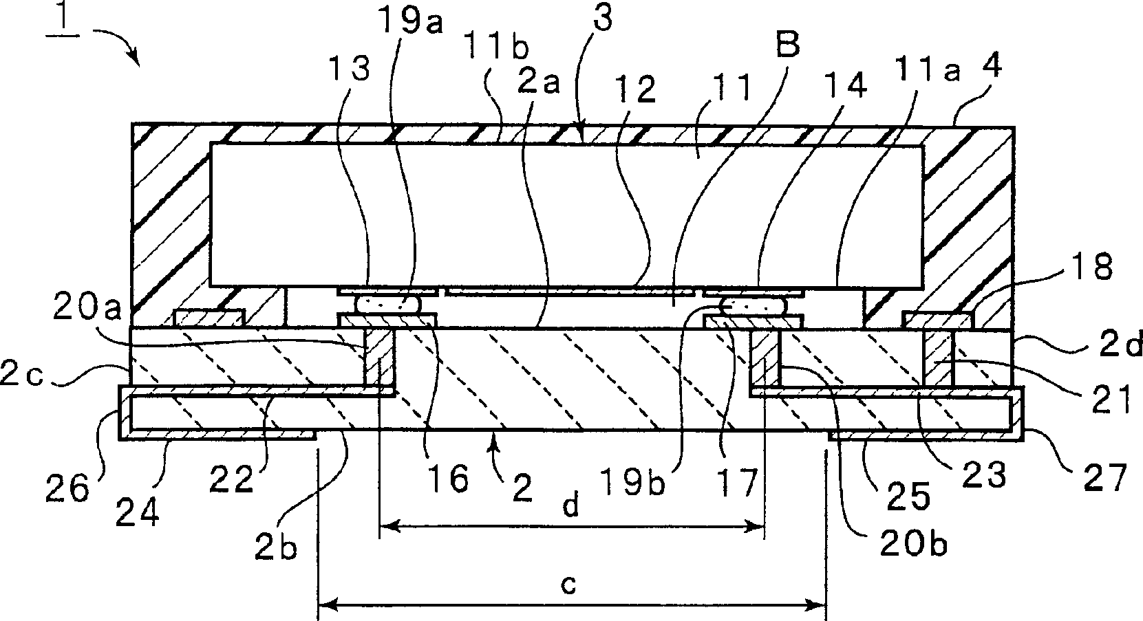
[0084] figure 1 is a cross-sectional view of the surface acoustic wave device according to the first embodiment of the present invention. The surface acoustic wave device 1 has a multilayer substrate 2 and a surface acoustic wave element 3 bonded to the multilayer substrate 2 by bumps. The periphery of the surface acoustic wave element 3 is covered with a resin sealing layer 4 .

[0085] The surface acoustic wave element 3 has a surface wave substrate 11 . The surface wave substrate 11 is constituted by a voltage substrate, a structure in which a piezoelectric thin film is laminated on an insulating substrate, or a structure in which a piezoelectric thin film is further laminated on a piezoelectric substrate.

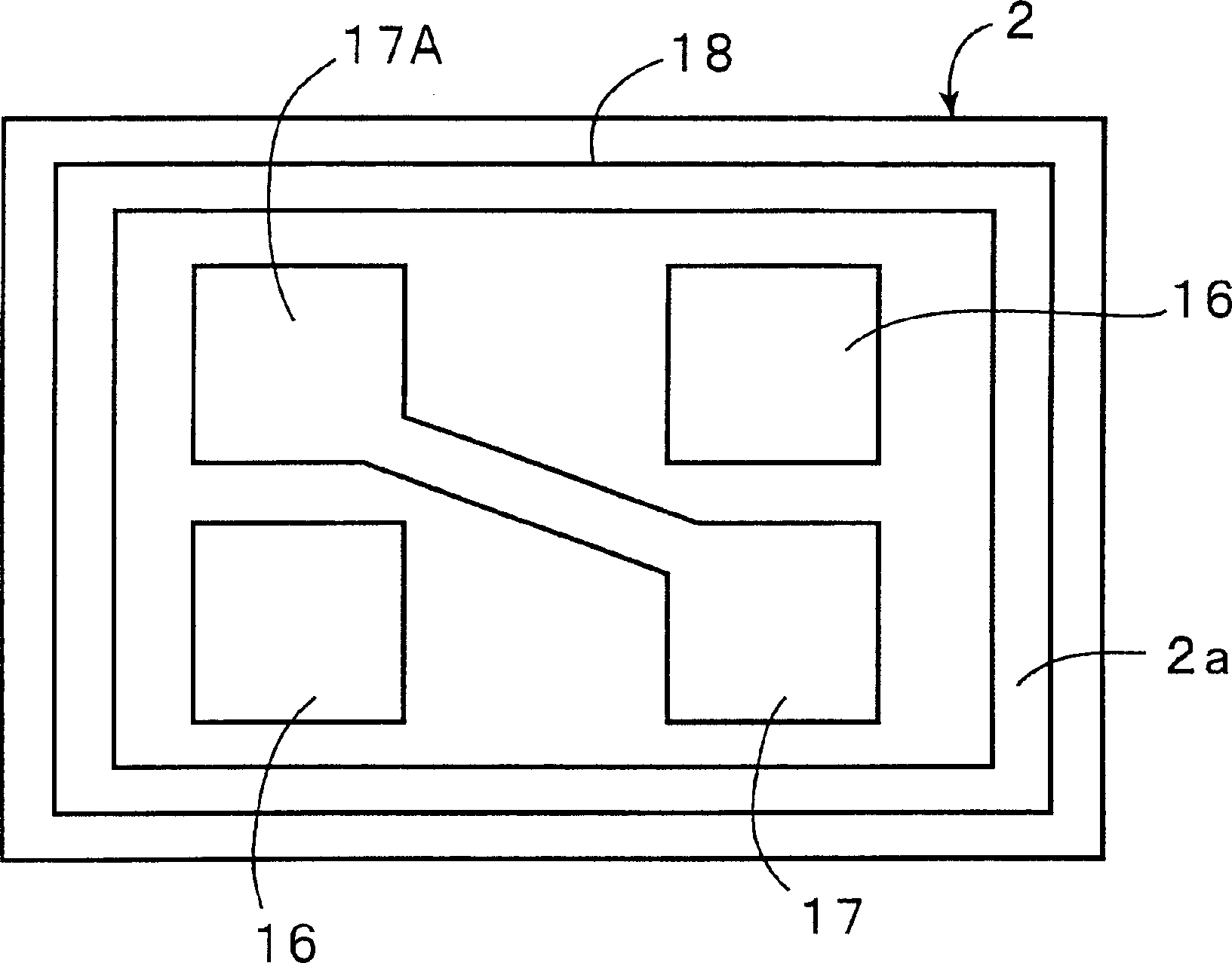
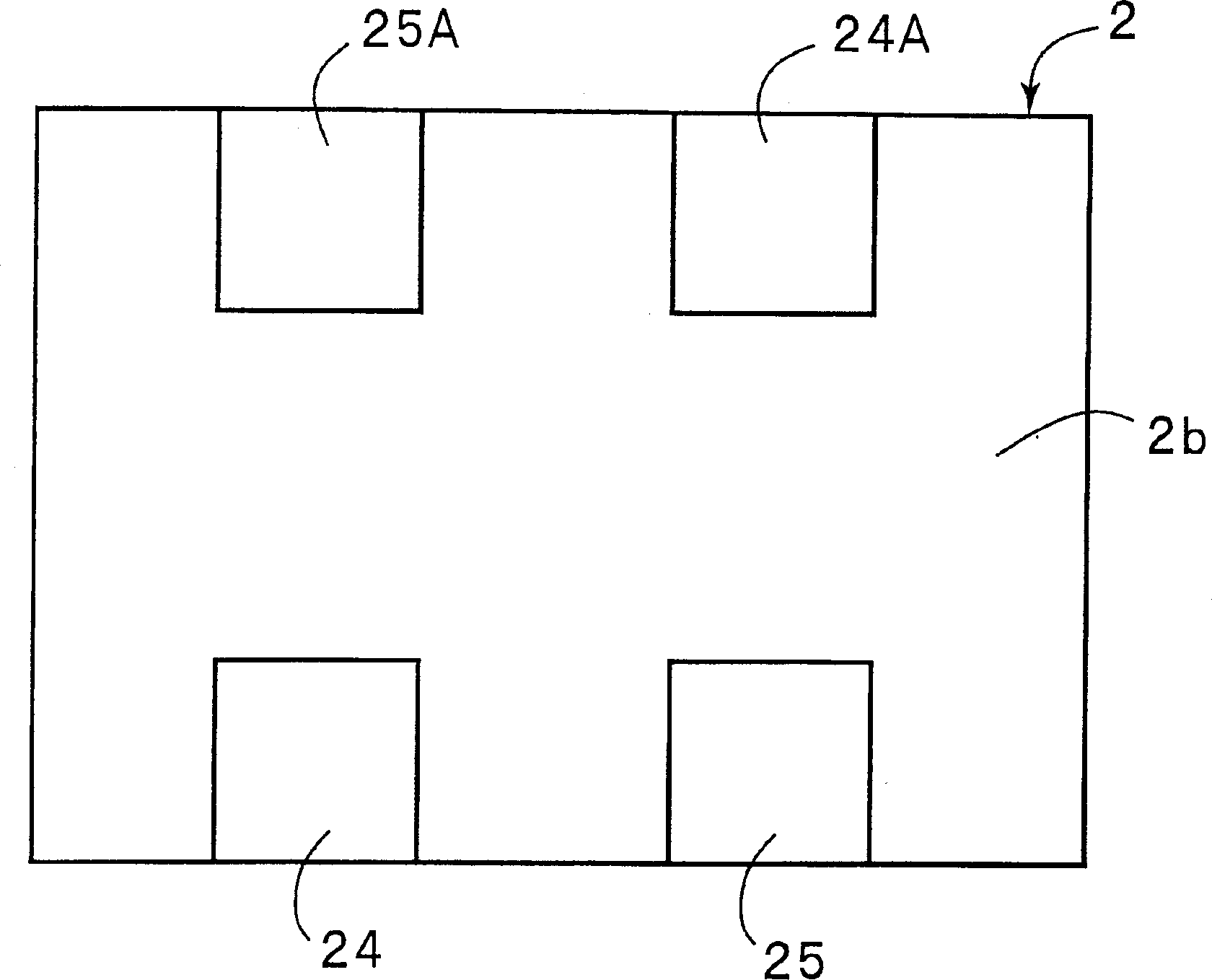
[0086] The surface wave substrate 11 has first and second main surfaces 11a and 11b. Electrod...


PUM


Abstract

A surface acoustic wave device which hardly causes short- circuit between mounting electrodes in mounting of an elastic surface wave element, even devised to be miniaturized, and facilitates checking the formation of fillets of a conductive bond in mounting, thus reducing the cost, with the element being mounted on a board and sealed with a resin-sealing layer. The surface acoustic wave device 1 has a surface acoustic wave element 3, which is mounted on a multilayer board 2 by the face down method using bumps 19a, 19b and sealed with a resin-sealing layer 4. Electrode lands 16, 17 on the upper side 2a of the multilayer board 2 connected to the bumps 19a, 19b are connected to inner electrodes 22, 23 via electrodes 20a, 20b, and the inner electrodes 22, 23 are electrically connected to mounting electrodes 24, 25 on the lower side of the board 2 and to end-face wiring electrodes 26, 27.

Description

technical field [0001] The present invention relates to a surface acoustic wave device having a structure in which a surface acoustic wave element is bonded to a substrate by a flip-chip method, and more particularly relates to a surface acoustic wave element stack and a surface acoustic wave device having an improved substrate structure. Background technique [0002] Conventionally, the miniaturization and low profile of surface acoustic wave devices housing surface acoustic wave elements have been strongly pursued. For this reason, the surface acoustic wave element employs bump bonding on the substrate with the surface on which the electrode for the surface acoustic wave element such as IDT is formed as the lower surface. A structure in which a surface acoustic wave element is mounted on a substrate by a so-called flip-chip method has been proposed. [0003] In addition, a surface acoustic wave device storing a surface acoustic wave element is required to have an airtight...

Claims


Application Information

Patent Timeline
Patent Type & Authority Applications(China)
IPC IPC(8): H03H9/145H01L41/08H03H9/25H01L41/053
CPCH01L2924/15192H03H9/059H01L23/3121H01L2924/15174H01L2924/01079H03H9/1085H01L2924/3025H01L2224/16H01L23/315H01L2224/05568H01L2224/05573
Inventor 馬場俊行大村正志
Owner MURATA MFG CO LTD
Why Eureka
Try Eureka