Practical assembling method for microcylinder lens and optical fibre

A technology of micro-cylindrical lens and assembly method, which is applied in the coupling of optical waveguides and other directions, and can solve problems such as large optical power coupling loss

Inactive Publication Date: 2003-08-06
INST OF SEMICONDUCTORS - CHINESE ACAD OF SCI
View PDF0 Cites 5 Cited by
  • Summary
  • Abstract
  • Description
  • Claims
  • Application Information

AI Technical Summary

Problems solved by technology

Usually, the mode field of the semiconductor laser does not match the mode field of the single-mode fiber, so when the

Method used


Image

  • Practical assembling method for microcylinder lens and optical fibre
  • Practical assembling method for microcylinder lens and optical fibre
  • Practical assembling method for microcylinder lens and optical fibre

Examples


Embodiment Construction

[0020] For the difficulties faced in the above several situations, an effective solution is to process a micro-lens of a certain shape on the end of the optical fiber. The micro-lens makes the mode field of the semiconductor laser match the mode field of the optical fiber, so that we can obtain Satisfactory coupling efficiency.

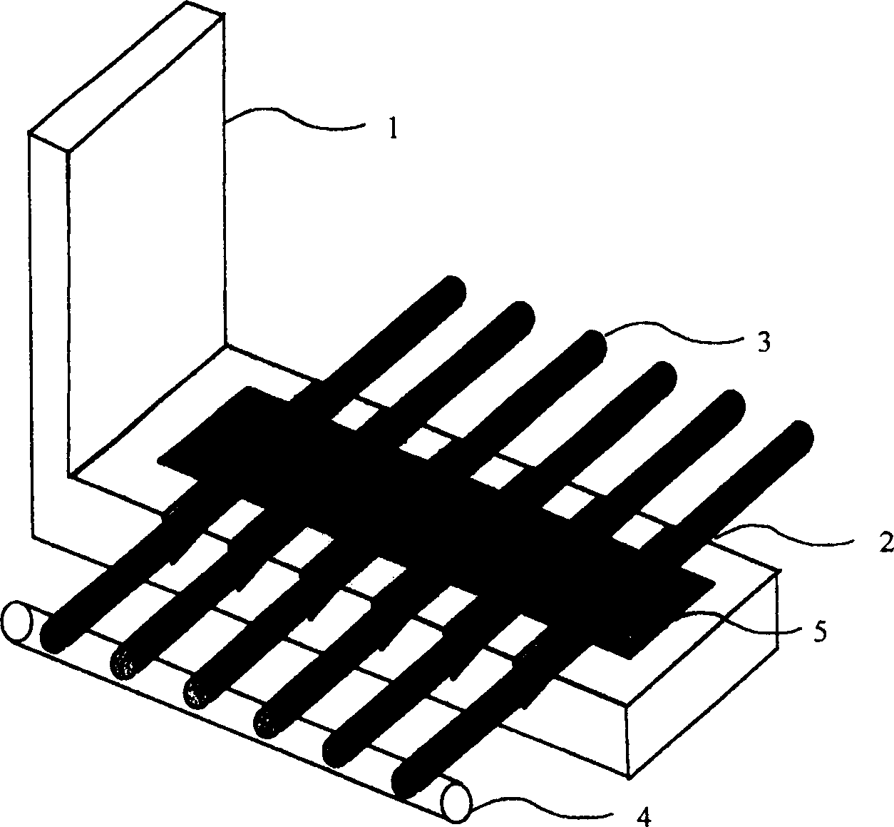
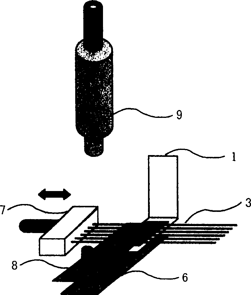
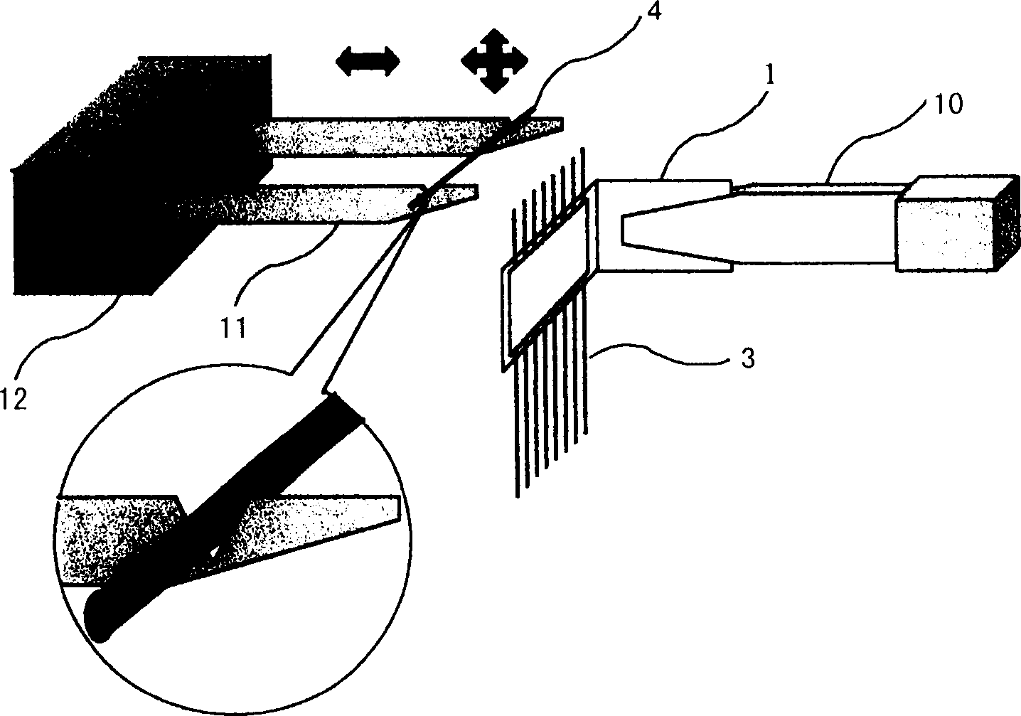
[0021] First, use a fiber cleaver to cut out an optical fiber with a flat end surface and a mirror surface for future use. exist figure 1 On the L-shaped bracket 1 shown, equidistant V-shaped grooves 2 are engraved by precision machining. The distance between the V-shaped grooves 2 should be equal to the distance between the semiconductor laser array light-emitting units to be coupled with it. The number of 2 is at least two more than the total number of light emitting units of the semiconductor laser array. After the V-shaped groove 2 is engraved, insert the cut optical fibers into the V-shaped groove 2 one by one, cover the top with a cover plate ...


PUM


Abstract

The invention is a practical assembling method of micro-cylinder lens and fibre-optical, including the steps: 1) firstly cut out the fibre-optical with smooth end surface; 2). on L-shaped bracket, carve out V-shaped slots with equal spaces; 3) insert the cut fibre-optical in V-shaped slots one by one, and place top cover plate on them and clamp the top cover plate inserted with fibre-optical array together with the L-shaped bracket; 4) on one side of fibre-optical end surface, use a smooth mobile sliding block controlled by trimmer rack to lean lightly against the array to make the end surface of the array on a same plane; 5) use adhesives to glue the L-shaped bracket together with the top cover plate; 6) install micro-cylinder lens on the end surface of the array.

Description

technical field [0001] The invention relates to a practical assembly method of a micro-cylindrical lens and an optical fiber, which can greatly simplify the coupling optical system of an optical fiber (optical fiber line array) and a semiconductor laser, while maintaining high coupling efficiency. Background technique [0002] In the semiconductor laser end-pumped all-solid-state laser technology, the high-power semiconductor laser used as the pump source must efficiently couple the emitted laser light into the transmission fiber. On the one hand, the active layer of high-power semiconductor lasers is very thin, usually less than 1 micron, and in order to obtain high power output, the width of the active layer is often very large, for example, for a semiconductor laser with an output power of 1 watt, the width of the active layer The width of the active layer of a semiconductor laser with an output of 2 watts is 100 microns, and the width of the active layer is 200 microns. ...

Claims


Application Information

Patent Timeline
IPC IPC(8): G02B6/32
Inventor 陈少武
Owner INST OF SEMICONDUCTORS - CHINESE ACAD OF SCI
Why Eureka
Try Eureka