Photomask for off-axis illumination and its producing method

A technology of photomask and external irradiation, which is applied in the field of photomask and its manufacturing, and can solve problems such as separation

Inactive Publication Date: 2003-08-20
SAMSUNG ELECTRONICS CO LTD
View PDF0 Cites 19 Cited by
  • Summary
  • Abstract
  • Description
  • Claims
  • Application Information

AI Technical Summary

Problems solved by technology

[0013] A second object of the present invention is to provide a method of manufacturing a photomask suitable for mass production by solving the conventional problems of detaching and reattaching a grating mask on the backside of the photomask

Method used


Image

  • Photomask for off-axis illumination and its producing method
  • Photomask for off-axis illumination and its producing method
  • Photomask for off-axis illumination and its producing method

Examples


Embodiment Construction

[0031] The present invention will now be described more fully with reference to the accompanying drawings, in which preferred embodiments of the invention are shown. However, this invention may be embodied in many different forms and should not be construed as limited to the embodiments set forth herein. Rather, these embodiments are provided so that this disclosure will be thorough, and will fully convey the scope of the invention to those skilled in the art. In the drawings, the configuration of elements is exaggerated for clarity. Like reference numbers refer to like elements throughout the drawings.

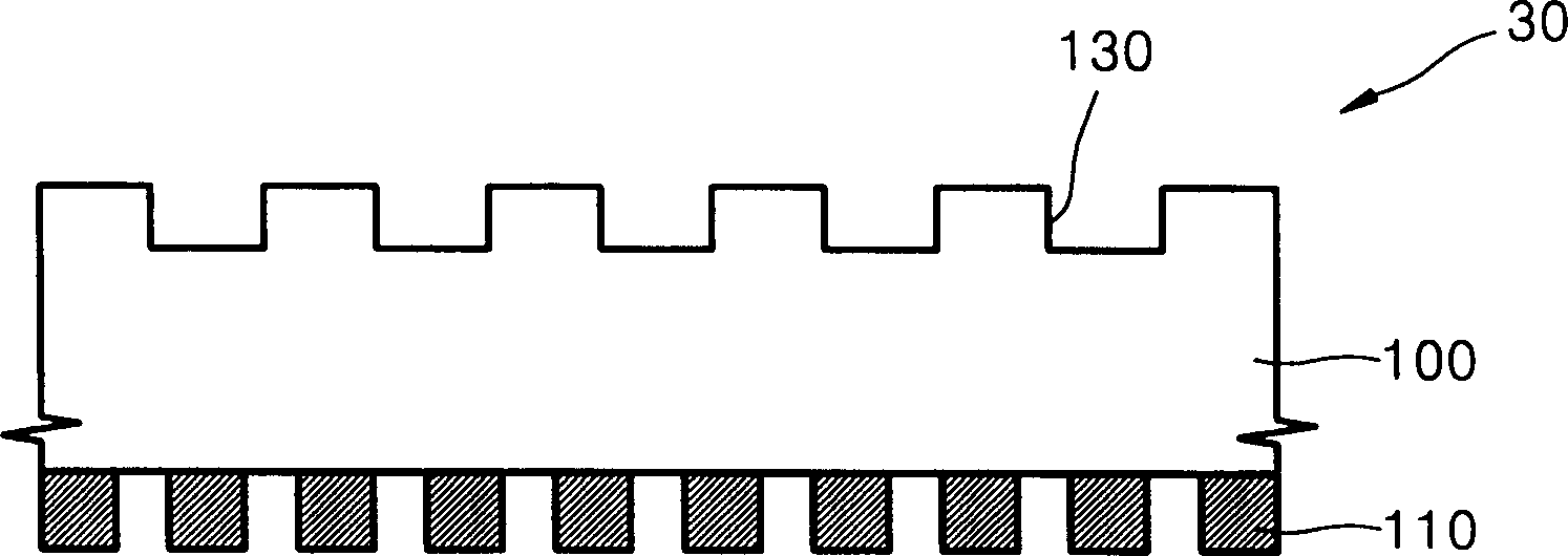
[0032] image 3 and 4 are cross-sectional views of photomasks according to first and second embodiments of the present invention, respectively.

[0033] refer to image 3 , the photomask 30 according to the first embodiment of the present invention is formed on the transparent substrate 100 . The transparent substrate 100 is formed of glass or quartz. A plurality of opaq...


PUM


Abstract

A photomask (50) comprises a transparent substrate; opaque patterns formed on a front surface of the substrate; and phase gratings (150) formed on a back surface of the substrate, allowing off-axis illumination (OAI) of an incident light source beyond an OAI limit of an exposure equipment. A photomask comprises a transparent substrate; opaque patterns formed on a front surface of the substrate, for defining a floodlighting portion for forming patterns; and phase gratings formed on a back surface of the substrate, allowing OAI of an incident light source beyond an OAI limit of exposure equipment, allowing use in an outmost region of an aperture and allowing modified illumination having a shape suitable for a layout of the opaque patterns. An independent claim is also included for a method of fabricating a photomask comprising forming opaque patterns for defining a floodlighting portion for forming patterns, on a front surface of a substrate; and forming phase gratings on a back surface of the substrate.

Description

technical field [0001] The present invention relates to a photomask for manufacturing a semiconductor device and a method of manufacturing the same, and more particularly, to a photomask for off-axis illumination (OAI) on which a phase grating is formed, and a method of manufacturing the same. Background technique [0002] A photomask image or pattern defining various features is focused on photoresist with light in a photolithographic process. To achieve tiny features, a finer image must be brought into focus on the photoresist, and optical resolution must be increased. However, there is a limit to the resolution that can be achieved. [0003] Thus, in order to manufacture semiconductor devices close to the resolution limit of lithographic processes, resolution enhancement techniques must be used. Resolution enhancement techniques include a method using a light source with a wavelength smaller than that in the prior art, a method using a phase shift mask, and a method usi...

Claims


Application Information

Patent Timeline
Patent Type & Authority Applications(China)
IPC IPC(8): G03F1/26G03F1/68G03F1/76G03F1/78G03F1/80G03F7/20H01L21/027
CPCG03F1/144G03F7/70125G03F1/34G03F1/50H01L21/027
Inventor 申仁均孙正玟尹熙璇崔成云
Owner SAMSUNG ELECTRONICS CO LTD
Why Eureka
Try Eureka