

Signal processing device and D/A converter
A signal processing device and converter technology, which is applied to digital-to-analog converters, recording signal processing, analog-to-analog conversion, etc., to achieve the effect of reducing the processing bit width and circuit area
- Summary
- Abstract
- Description
- Claims
- Application Information
AI Technical Summary
Problems solved by technology
Method used
Image

Examples
no. 1 Embodiment approach
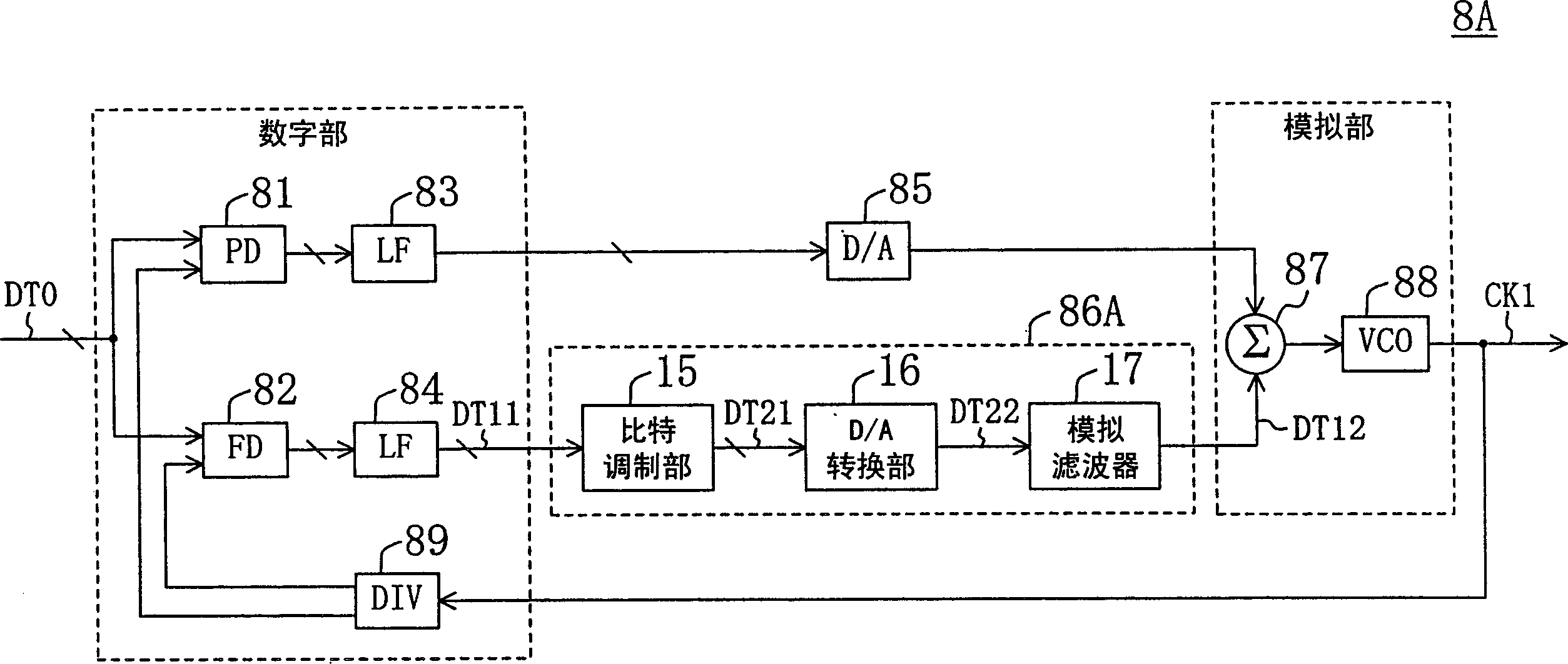
[0050] figure 2 The configuration of the PLL block 8A according to the first embodiment of the present invention is shown. The PLL block 8A of this embodiment is equipped with a D / A converter 86A instead of Figure 15 The D / A converter 86.
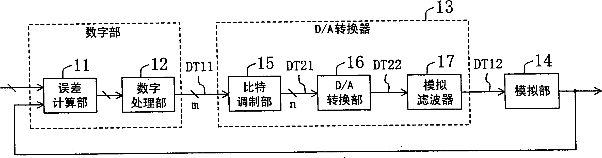
[0051] The PLL block 8A includes: a phase comparator 81; a frequency comparator 82; a digital filter 83 that outputs an 8-bit digital control signal after smoothing the phase error; a digital filter 83 that outputs an 8-bit digital control signal DT11 after smoothing the frequency error filter 84; D / A converters 85, 86A; an adder 87 that adds the outputs of the D / A converters 85, 86A; a VCO 88 that changes the oscillation frequency of the output clock CK1 according to the output of the adder 87 and outputs A frequency divider 89 for generating a frequency-divided clock after frequency division of the clock CK1 . In addition, the comparators 81, 82 and the digital filters 83, 84 correspond to the digital part of the present invention, a...
no. 2 Embodiment approach
[0070] Image 6 The configuration of the PLL block 8B according to the second embodiment of the present invention is shown. The PLL block 8B of the present embodiment includes a D / A converter 86B instead of the D / A converter 86A in the PLL block 8A of the first embodiment. Hereinafter, the D / A converter 86B will be described in detail.
[0071] D / A converter 86B is composed of bit modulation unit 15A, D / A conversion unit 16 , analog filter 17 , current source 20 , and adder 21 . In addition, the current source 20 corresponds to the power supply unit of the present invention.
[0072] Figure 7 The configuration of the bit modulation unit 15A is shown. The bit modulation unit 15A outputs a 7-bit signal DT21 and a 1-bit modulation bit DT23 based on the input digital control signal DT11 .
[0073] The output of the register 151 is a 7-bit signal DT21 output from the bit modulation unit 15A. Therefore, the signal DT21 outputs the upper 7 bits of the digital control signal DT...
no. 3 Embodiment approach
[0080] Figure 10 The configuration of the PLL block 8C according to the third embodiment of the present invention is shown. The PLL block 8C of the present embodiment includes a D / A converter 86C instead of the D / A converter 86A in the PLL block 8A of the first embodiment.
[0081] Generally, the variable range of the oscillation frequency of the VCO 88 controlled in the phase loop (81-83A-85-87-88-89) is the same as that of the frequency loop (82-84A-86C-87-88-89). Very narrow compared to the variable range. For example, the output range of the D / A converter 85 of the phase loop is set to about 10% of the output range of the D / A converter 86C of the frequency loop.
[0082] However, in recording media such as CDs, the recording frequency differs between the inner and outer discs. When reproducing a signal recorded on such a medium, the frequency of the reproduced data changes slowly after the phase loop becomes stable. Therefore, in the phase loop, it is necessary to slo...
PUM
 Abstract
Description
Claims
Application Information