Flash memory structure and mfg method thereof

A manufacturing method and flash memory technology, which are applied in semiconductor/solid-state device manufacturing, electrical components, electrical solid-state devices, etc., and can solve problems such as inability to perform more precise control.

Inactive Publication Date: 2003-10-22
WINBOND ELECTRONICS CORP
View PDF0 Cites 7 Cited by
  • Summary
  • Abstract
  • Description
  • Claims
  • Application Information

AI Technical Summary

Problems solved by technology

[0012] In view of the above-mentioned background of the invention, the flash memory formed according to the traditional technology needs to use at least...

Method used


Image

  • Flash memory structure and mfg method thereof
  • Flash memory structure and mfg method thereof
  • Flash memory structure and mfg method thereof

Examples


Embodiment Construction

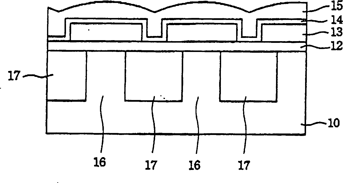
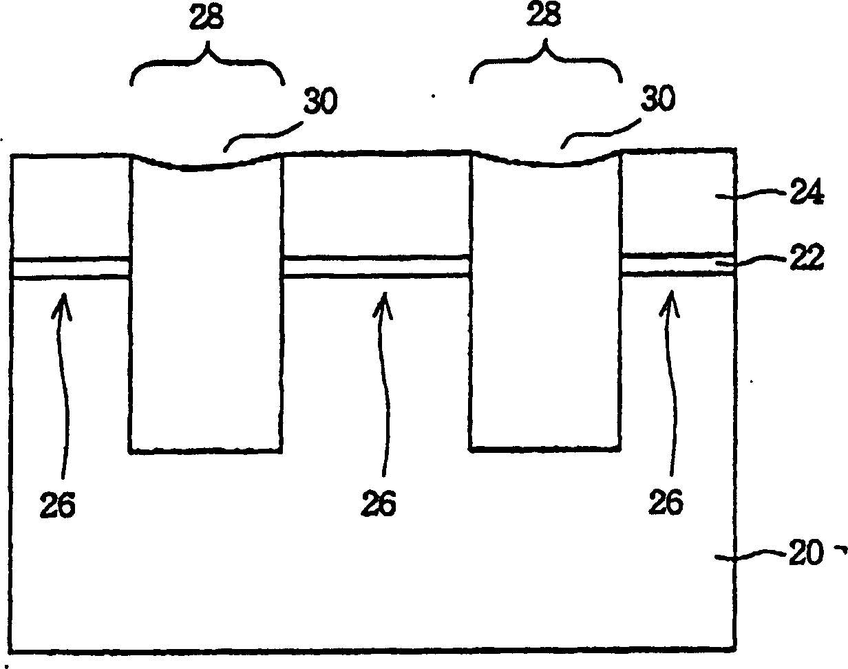
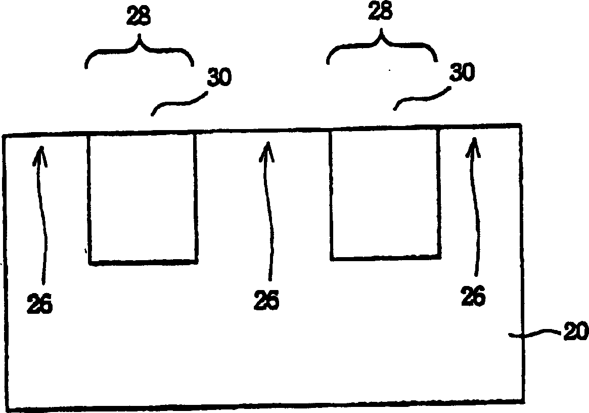
[0065] Without limiting the spirit and scope of application of the present invention, the implementation of the present invention is introduced below with an embodiment; those of ordinary skill in the art, after understanding the spirit of the present invention, can apply the method of the present invention for each A different method of flash memory is used to eliminate the traditional defect that alignment errors often occur during mask alignment due to the need to use at least two different masks to form the floating gate layer and the active region. At the same time, the flash memory structure of the present invention can increase the coupling area between the floating gate layer and the control gate layer without sacrificing the total area of ​​the flash memory, so as to increase the cross-connection capacitance therebetween. The application of the present invention should not be limited to the embodiments described below.

[0066] As described in the background of the in...


PUM

PropertyMeasurementUnit
Depthaaaaaaaaaa

Abstract

This invention relates to a flash structure and its processing method in which, the finished flash suspended grating does not need microimage method, so situation of mistaken aligning will not occur between the suspended grating layer and the active zone, utilizing etching channel insulation zone to reach convex structure and its only necessary to add the etching depth of channel isolation area to increase the couple area between suspending grating layer and controlling grating to increase their cross link capacity without sacrificing flash total area.

Description

technical field [0001] The present invention relates to a storage device, in particular to a flash memory (Flash memory) structure and a manufacturing method thereof. The flash memory structure is self-aligned. Background technique [0002] When the function of the computer microprocessor becomes stronger and stronger, the data calculation performed by the software becomes larger and larger, and of course the demand for memory is also higher. Therefore, the development of higher integration means the generation of memory with larger capacity. When Intel developed "Flash memory" (Flash memory) with the same structure as Electrically Erasable Programmable ROM (EEPROM) in the late 1980s, because data can be stored, read and cleared multiple times, so Become the fastest growing new generation of memory. [0003] Non-volatile memory, especially flash memory, is gaining importance in a variety of applications. In recent years, the demand for flash memory has been gradually high...

Claims


Application Information

Patent Timeline
IPC IPC(8): H01L21/8239H01L27/10
Inventor 张文岳
Owner WINBOND ELECTRONICS CORP
Why Eureka
Try Eureka