Phase transformation memory and manufacturing method thereof

A manufacturing method and phase change technology, which are applied in the field of memory, can solve the problems of difficulty in controlling the thickness and doping concentration of N+ doped regions and N- doped regions, prone to breakdown, and difficult to shrink in size, etc.

Inactive Publication Date: 2003-11-12
MACRONIX INT CO LTD
View PDF0 Cites 1 Cited by
  • Summary
  • Abstract
  • Description
  • Claims
  • Application Information

AI Technical Summary

Problems solved by technology

[0003] The thickness and doping concentration of the N+ doped region and N- doped region in the above-mentioned traditional phase change memory structure are difficult to control, so that the breakdown voltage (BDV) cannot be adjusted
And adjacent P+ / P+ intervals and adjacent word lines / word lines are prone to breakdown (punch)
Therefore, the component size is not easily reduced

Method used


Image

  • Phase transformation memory and manufacturing method thereof
  • Phase transformation memory and manufacturing method thereof
  • Phase transformation memory and manufacturing method thereof

Examples


Embodiment Construction

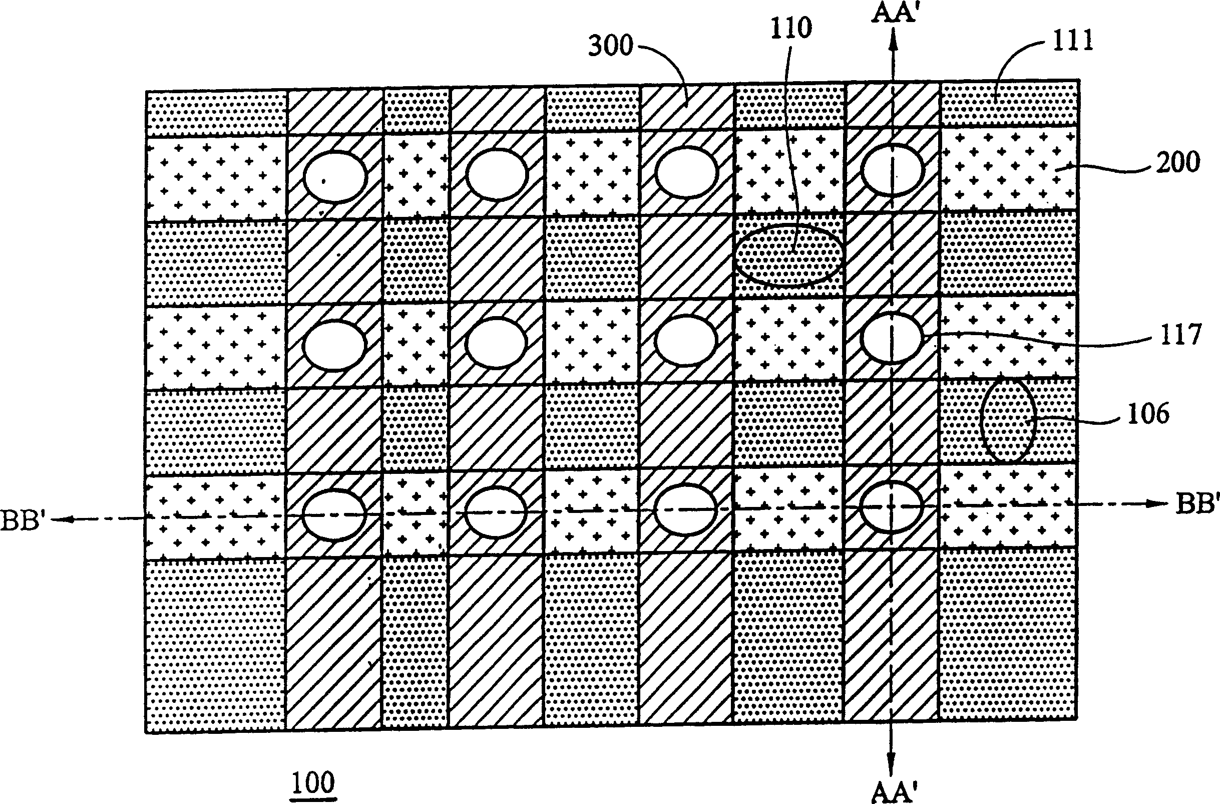
[0011] First, please refer to figure 2 , showing a top view of a phase change memory structure according to an embodiment of the present invention. The phase change memory structure includes a semiconductor substrate 100; an insulating layer 111 is formed on the semiconductor substrate 100, and the insulating layer 111 can be an oxide layer. The phase change memory structure includes a P+ doped region 117 , a word line 200 , a bit line 300 , a first shallow trench isolation structure 106 , and a second shallow trench isolation structure 110 .

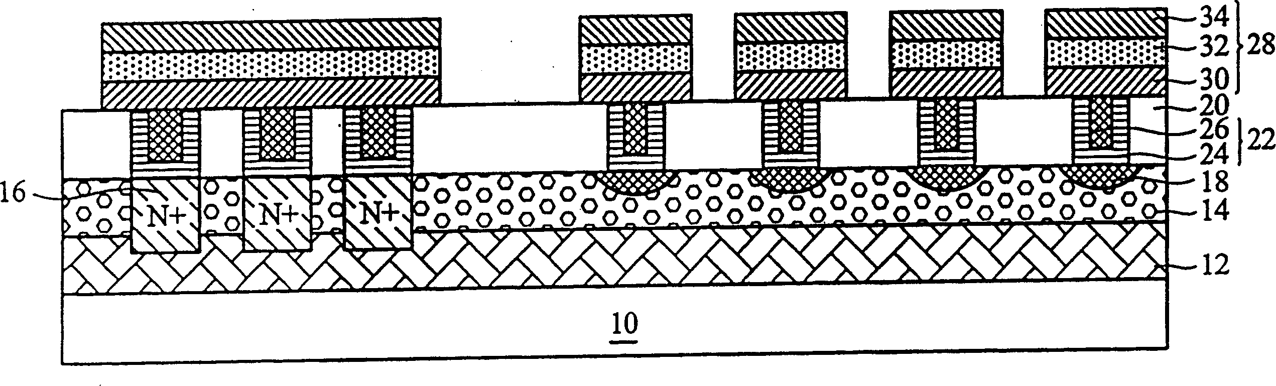
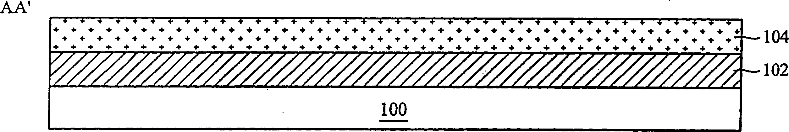
[0012] Figure 3 to Figure 4 show based on figure 2 The AA' profile, Figure 5 to Figure 8 show based on figure 2 The BB' profile. Please refer to image 3 , the embodiment of the present invention firstly provides a semiconductor substrate 100 , an N+ epitaxial layer 102 and an N− epitaxial layer 104 are successively formed on the semiconductor substrate 100 . The N+ epitaxy layer 102 and the N- epitaxy layer 104 can be forme...


PUM


Abstract

First, an N+polycrystal layer and an N- polycrystal layer are formed on a semiconductor substrate. The first shallow-channel isolation structure is formed in the N+ layer in order to isolate the prearranged character line region; and the second shallow-channel isolation structure is formed in the N- layer in order to isolate the prearranged P+ adulteration region. Next, the defined insulation layer is formed. N+ adulterating is carried out for the part of N- polycrystal layer in order to connect N+ adulteration region in N+ polycrystal layer. P+ is adulterated in the N+ polycrystal layer so as to form a P+ adulteration region. The, the contact plug across the insulation layer is formed on the N+ adulteration region and the P+ adulteration region respetively. Finally, an upper electrode, a phase change layer and a lower electrode are formed on the contact plug being as an electrod.

Description

technical field [0001] The invention relates to a memory, in particular to a phase-change memory and a manufacturing method thereof. Background technique [0002] figure 1 To show the traditional phase change memory structure. The phase change memory structure includes a semiconductor substrate 10, an N+ doped layer 12 formed on the semiconductor substrate 10, an N-doped layer 14 formed on the N+ doped layer 12, and an N+ doped region 16 formed on the In the N-doped layer 14, a P+ doped region 18 is formed in the N-doped layer 14, and an insulating layer 20 is formed on the semiconductor substrate 10, and the insulating layer 20 can be an oxide layer. The contact plug 22 includes a barrier layer 24 and a metal layer 26 . The electrodes 28 are respectively formed on the contact plugs 22 , and the electrodes 28 have an upper electrode 34 , a phase change layer 32 and a lower electrode 30 . [0003] The thickness and doping concentration of the N+ doped region and the N− do...

Claims


Application Information

Patent Timeline
Patent Type & Authority Applications(China)
IPC IPC(8): H01L21/82H01L21/8239H01L27/04
Inventor 刘慕义范左鸿詹光阳叶彦宏卢道政
Owner MACRONIX INT CO LTD
Why Eureka
Try Eureka