

Plane internal switch mode active matrix liquid crystal display device and mfg. method thereof
A switch-mode and active-matrix technology, which is applied in the field of in-plane switch-mode active-matrix liquid crystal display devices and its manufacture, can solve problems such as spots on the display screen, and achieve the effect of expanding the display area and reducing the area
- Summary
- Abstract
- Description
- Claims
- Application Information
AI Technical Summary
Problems solved by technology
Method used
Image

Examples
no. 1 example
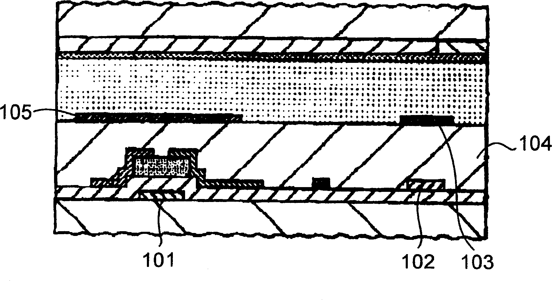
[0060] image 3 , 4 , 5 represent the in-plane switching mode active matrix type liquid crystal display device according to the first embodiment of the present invention. image 3 is a plan view of an active matrix liquid crystal display device 10 according to a first embodiment of the present invention, Figure 4 is along image 3 The sectional view taken on line IV-IV, Figure 5 is like image 3 A circuit diagram of one pixel of the liquid crystal display device 10 is shown.
[0061] Such as Figure 4 As shown, the liquid crystal display device 10 includes: an active device substrate 11 , an opposite substrate 12 , and a liquid crystal layer 13 sandwiched between the active device substrate 11 and the opposite substrate 12 .
[0062] The opposite substrate 12 includes: an electrically insulating transparent substrate 16, a black matrix layer 17 used as a light-shielding film formed in a matrix form on the electrically insulating transparent substrate 16, formed on the ...
no. 3 example
[0179] Figure 19 is a sectional view of a liquid crystal display device 50 according to a third embodiment of the present invention.
[0180] In the liquid crystal display device 50 according to the third embodiment of the present invention, the pixel electrode 25 is made of ITO similarly to the second embodiment, and the transparent body 25a serves as a protective layer covering the data line 24 . The structure of the liquid crystal display device 50 according to the third embodiment of the present invention is the same as that of the liquid crystal display device 40 according to the above-mentioned second embodiment of the present invention except that the data line 24 is covered with the transparent body 25a.
[0181] Similar to the pixel electrode 25 , the transparent electrode 25 a is composed of ITO, and is formed simultaneously with the pixel electrode 2 . Since the transparent electrode 25a can be formed by partially changing the pattern used to form the pixel electr...
no. 4 example
[0184] Figure 20 is a sectional view of an in-plane switching mode active matrix type liquid crystal display device 60 according to a fourth embodiment of the present invention.
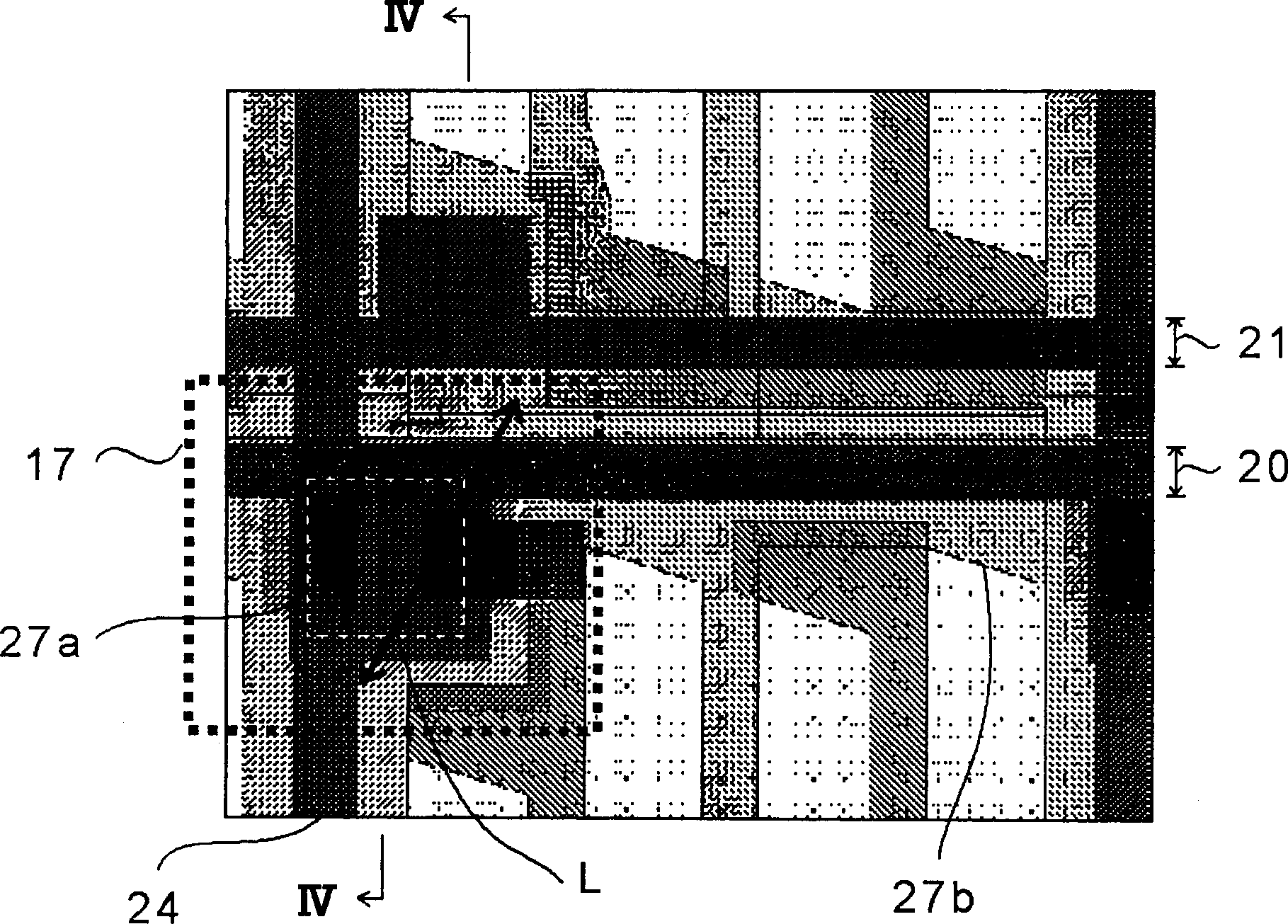
[0185] In the liquid crystal display device 10 according to the first embodiment of the present invention, the black matrix layer 17 is formed as a part of the opposing substrate 12, as Figure 4 shown. In contrast, the black matrix layer 17a in the liquid crystal display device 60 according to the fourth embodiment of the present invention is formed as a part of the active device substrate 11.
[0186] The black matrix layer 17a blocks the opening 27a of the common electrode 27 and is only formed above the thin film transistor 30 so that the black matrix layer 17a overlaps the thin film transistor 30, which is similar to the first embodiment. That is, the black matrix layer 17 a has a minimum size necessary for preventing light from entering the thin film transistor 30 . In addition, the black m...
PUM
| Property | Measurement | Unit |
|---|---|---|
| electrical resistivity | aaaaa | aaaaa |
| electrical resistivity | aaaaa | aaaaa |
| thickness | aaaaa | aaaaa |
Abstract
Description
Claims
Application Information