Electrooptical device and electronic instrument

An electro-optical device and pixel electrode technology, which is applied in the direction of instruments, electric light sources, identification devices, etc., can solve the problems of difficult planarization of the insulating film 183, and achieve the effects of ensuring insulation, suppressing differences in insulation, and improving uniformity

Inactive Publication Date: 2003-12-10
SEIKO EPSON CORP
View PDF0 Cites 2 Cited by
  • Summary
  • Abstract
  • Description
  • Claims
  • Application Information

AI Technical Summary

Problems solved by technology

However, since the second interlayer insulating film 176 and the first pixel electrode 181 are concave-convex, there is a problem that the insulating film 183 formed on the top of the pixel electrode 181 is difficult to be flattened.

Method used


Image

  • Electrooptical device and electronic instrument
  • Electrooptical device and electronic instrument
  • Electrooptical device and electronic instrument

Examples


Embodiment Construction

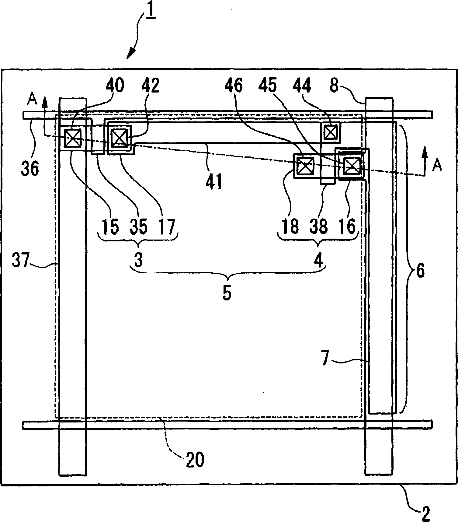
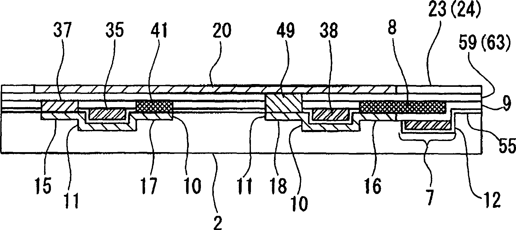
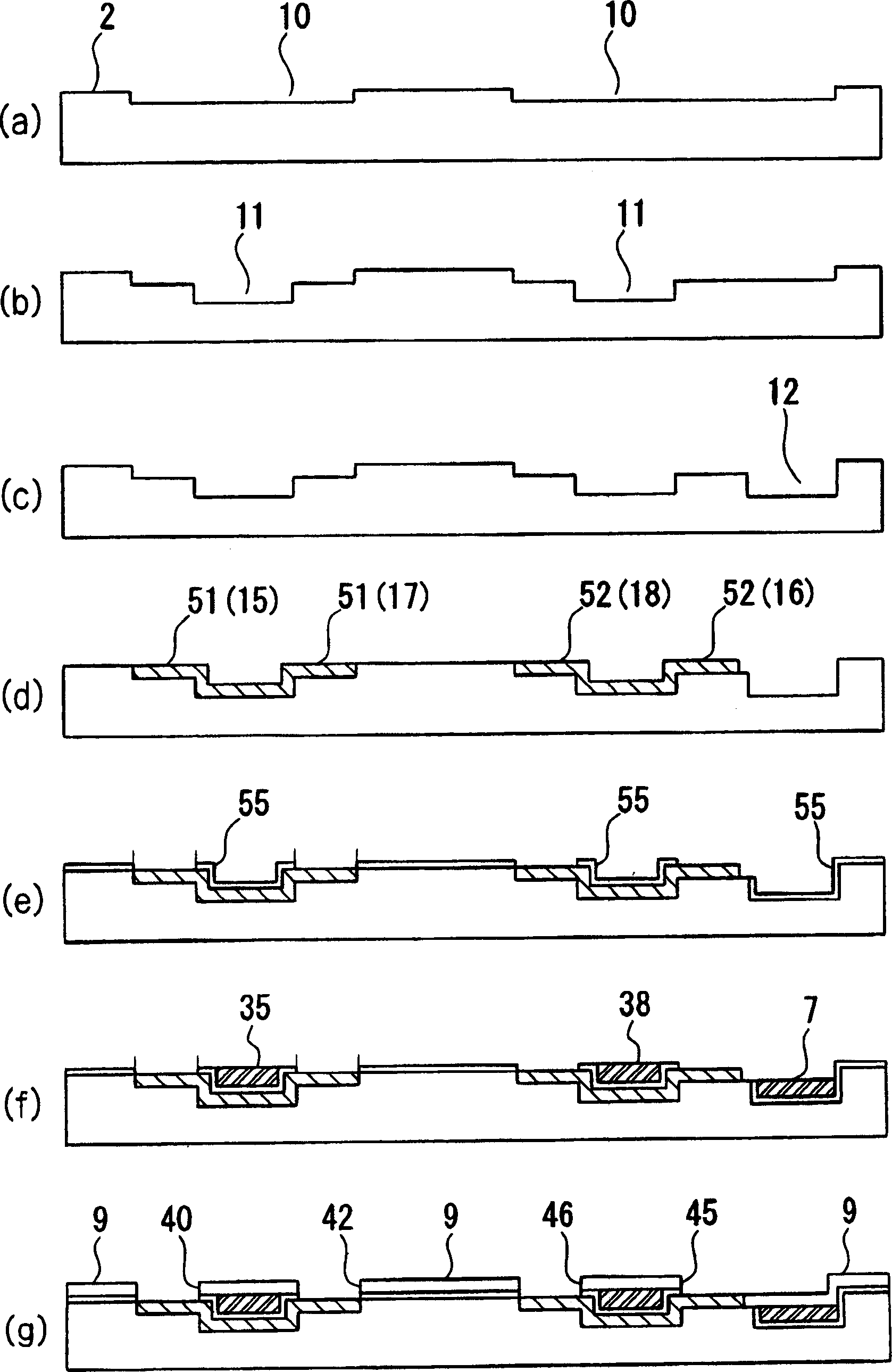
[0061] Hereinafter, embodiments of the present invention will be described with reference to the drawings. Figure 1 ~ Figure 6 It is a diagram illustrating an electro-optical device according to an embodiment of the present invention. figure 1 It is a plan view showing the main parts of the electro-optical device. figure 2 Yes means figure 1 A side sectional view of the A-A section. image 3 , Figure 4 It shows the manufacturing process of electro-optical devices figure 1 A side sectional view of the A-A section. Figure 5 It is a plan view of the electro-optical device. Figure 6 Yes means Figure 5 A side cross-sectional view of the B-B section.

[0062] The electro-optical device 1 of this embodiment is as figure 1 Shown are: a substrate 2, a switching element 5 composed of first and second TFTs 3 and 4 arranged on the substrate 2, a lower electrode 7 arranged under the holding capacitor 6 for holding image signals, and a lower electrode 7 arranged above the lower electr...


PUM


Abstract

The present invention is an electro-optical device having high aperture ratio, with which it is possible to easily planarize an insulating film stacked over a switching element, a wiring and an insulating film constituting the electro-optical device. The solution is to have an electro-optical device including a substrate 2, a switching element 5, a wiring 36 and an insulating film 21, 55 provided for the substrate 2. The substrate 2 comprises concave portions 10, 11, 12 corresponding to at least one position of the switching element 5, the wiring 36 and the insulating film 21, 55.

Description

Technical field [0001] The invention relates to an electro-optical device and an electro-optical device possessed by an electronic instrument. Background technique [0002] In recent years, there are a plurality of thin film transistors (TFT) on a substrate, and a plurality of organic EL elements driven by the thin film transistors and arranged corresponding to the thin film transistors (TFT). For organic active EL light-emitting devices, there is a structure proposal in which a planarized interlayer insulating film is arranged between the TFT and the lower electrode of the organic EL element. [0003] Picture 10 Shown is an example of an existing organic active light-emitting device. [0004] The organic active light-emitting device denoted by symbol 148 is composed of a plurality of thin film transistors (TFT) 150 formed on a substrate 149, an organic EL element 154 having a counter electrode 151, an organic layer 152, and a lower electrode 153, and an interlayer The insulati...

Claims


Application Information

Patent Timeline
Patent Type & Authority Applications(China)
IPC IPC(8): H05B33/02G02F1/1333G02F1/136G09F9/30H01L21/336H01L27/32H01L29/786H01L51/50H01L51/52H05B33/10H05B33/12H05B33/14H05B33/22
CPCH01L27/3262H01L27/3244H01L27/3246H01L51/52H10K59/1213H10K59/122H10K59/12H10K50/80H05B33/22
Inventor 茅野祐治
Owner SEIKO EPSON CORP
Why Eureka
Try Eureka