Ink jet device, ink and method of manufacturing electronic component using the device and the ink

The technology of an inkjet device and manufacturing method is applied in the direction of electrical components, conductive materials dispersed in non-conductive inorganic materials, circuits, etc., which can solve the problems of easy clogging of printing heads, easy clogging of printing heads, and inability to use them

Inactive Publication Date: 2003-12-17
PANASONIC CORP
View PDF32 Cites 22 Cited by
  • Summary
  • Abstract
  • Description
  • Claims
  • Application Information

AI Technical Summary

Problems solved by technology

Therefore, in conventionally proposed inkjet devices, inkjet printheads or ink ejection ports are prone to clogging, making it difficult to perform stable printing.
In addition, inkjet electronic component inks that can be printed stably use dyes or metal salts for coloring, etc., and cannot be used for the manufacture of electronic components such as LC filters and high-frequency components.
In addition, in the process of manufacturing laminated ceramic electronic components, even if you want to print electrode inks on ceramic sheets with a thickness of 20 μm or less, conventional inkjet devices cannot print inks for electronic components stably.
In this way, in the case of ink that is prone to sedimentation or re-agglomeration, conventional inkjet devices tend to clog inkjet printheads or ink outlets, making it difficult to perform stable printing, and no effective solution has been proposed.

Method used


Image

  • Ink jet device, ink and method of manufacturing electronic component using the device and the ink
  • Ink jet device, ink and method of manufacturing electronic component using the device and the ink
  • Ink jet device, ink and method of manufacturing electronic component using the device and the ink

Examples


Embodiment 1

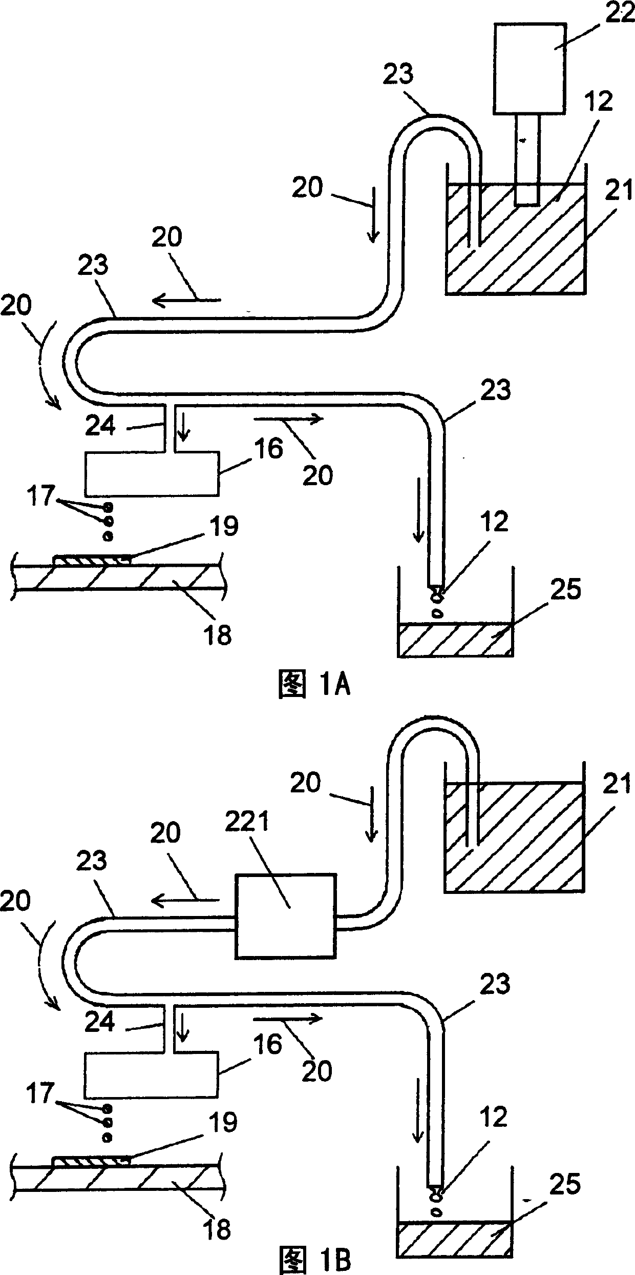
[0041] In Embodiment 1, an ink jet apparatus and an ink supply mechanism thereof according to an embodiment of the present invention will be described with reference to FIG. 1A . In FIG. 1A , the inside of the ink container 21 is filled with the ink 12 . And the disperser 22 re-disperses the ink 12 in the ink container 21 as needed. The ink in the ink container 21 flows into the ink recovery container 25 through the first pipe 23 by its own weight. In addition, by placing the ink container 21 at a position higher than the ink recovery container 25, the siphon principle can be utilized, and it is possible to flow naturally without using a pump or the like. In this way, the ink 12 in the ink container 21 is dropped into the ink recovery container 25 via the first tube 23 . In the present invention, the ink 12 always flows in the first tube 23, and only a required amount is sent to the print head 16 through the second tube 24 during printing. Then, the ink 12 filled in the pri...

Embodiment 2

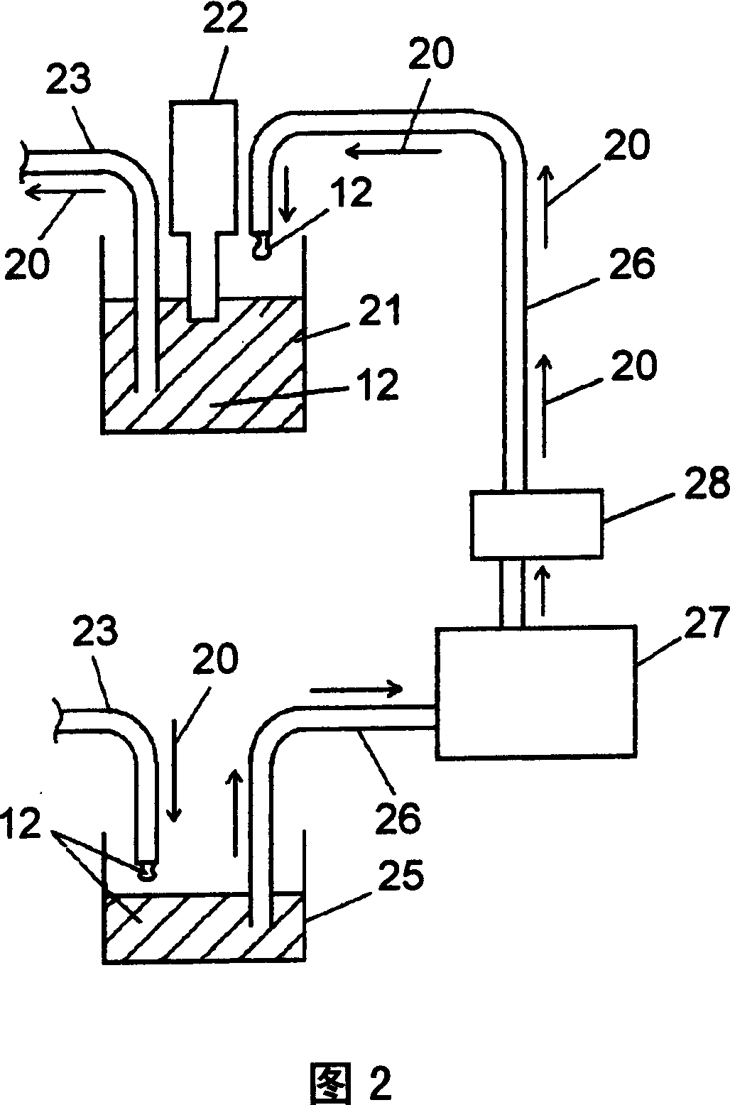
[0053] In Example 2, an example in which printing stability is further improved by removing fine air bubbles mixed into the ink will be described. We know that when a piezoelectric inkjet device is used on the print head 16, tiny air bubbles mixed in the ink will adhere and grow as air bubbles in the printer, absorb the vibration energy of the piezoelectric element, and prevent printing. Stable (for example, it is described in pages 202 to 206 of "Inkjet Printer Technology and Materials" (edited by Professor Takeshi Amari, Chiba University) published by CMC Corporation in 1998). In particular, in the present invention, since the disperser 22 is attached to the ink container 21, depending on the type of the disperser 22 (for example, a high-speed rotary homogenizer, an ultrasonic disperser, etc.), the ink container 21 may be Roll in tiny air bubbles. For example, there are cases in which air bubbles are entangled from the ink surface in a high-speed rotating homogenizer, or mi...

Embodiment 3

[0063] In Example 3, the characteristic of the present invention, ie, the circulation and dispersion of the ink, will be described in detail. FIGS. 6A and B are examples of actual measurement of the deposition rate of ink for electronic components. In particular, the ink for electronic components is extremely easy to agglomerate as described in FIGS. 16A and B and the like, so it is easy to precipitate. This is explained in further detail using FIGS. 6A and B. FIG. In FIG. 6A , the ink container 21 is filled with the ink 12, and the disperser 22 is immersed in the ink 12 in a state where the switch is OFF. In this way, if the ink is left to stand without using the disperser 22, as shown in FIG. 6A, as the elapsed time increases, a clear layer 36 is formed in the ink 12, and the thickness of the clear layer 36 increases with the elapsed time. FIG. 6B is a diagram illustrating the generation of clear layers of various inks for electronic components. In addition, although a cl...


PUM

PropertyMeasurementUnit
particle diameteraaaaaaaaaa

Abstract

The invention provides an inkjet device, an inkjet ink and an electronic element manufacturing method using the inkjet device and the inkjet ink. Use an inkjet device with ink circulation function and ink dispersion function to redisperse the used ink as needed, send a part of the ink to the print head during the delivery to the ink recovery container through the tube, and form a specified pattern on the surface of the printed object , even if it is an ink that is easy to precipitate and lacks printing stability, since the ink is redispersed in the ink container as needed, it can prevent ink from settling or agglomerating, and will not block the inkjet print head or ink outlet, thereby Stable inkjet printing can be realized and electronic components can be manufactured stably with high yield.

Description

technical field [0001] The present invention relates to a method for producing ceramic electronic components such as multilayer ceramic capacitors, high-frequency electronic components, filters, and multilayer substrates by performing stable non-contact printing with inkjet inks for various electronic component formation using an inkjet apparatus. method. Background technique [0002] Conventionally, the internal electrodes and ceramic layers of ceramic electronic components are often produced by a printing method using a plate, such as screen printing and gravure printing. Although these methods are suitable for mass production, they are not suitable for the multi-variety small-lot production in recent years. Therefore, as a new printing method, the use of inkjet in the manufacture of ceramic electronic components has been proposed. [0003] First, general inkjet inks will be described. General inkjet inks are dye-type or pigment-type. Since these types of inks will vola...

Claims


Application Information

Patent Timeline
Patent Type & Authority Applications(China)
IPC IPC(8): B41J2/175H01B1/16H01G4/00H05K3/12
CPCB41J2/175B41J2/17509
Inventor 中尾惠一沖中秀行
Owner PANASONIC CORP
Why Eureka
Try Eureka