Method for producing semi-conductor

A semiconductor and device technology, applied in the field of manufacturing semiconductor devices, can solve problems such as mask layer damage, infeasibility, and difficulty in conducting patterns

Inactive Publication Date: 2004-01-21
SK HYNIX INC
View PDF0 Cites 10 Cited by
  • Summary
  • Abstract
  • Description
  • Claims
  • Application Information

AI Technical Summary

Problems solved by technology

[0013] However, it is recommended to implement figure 1 In Korean Patent Application Laid-Open Publication No. 2000-0048819 of the shown method, it discloses the difficulty of forming each conductive pattern, for example, the silicon oxide layer spacers on the lateral sides of the bit lines, whose height is lower than that of the silicon nitride layer. to

Method used


Image

  • Method for producing semi-conductor
  • Method for producing semi-conductor
  • Method for producing semi-conductor

Examples


Embodiment Construction

[0053] Other objects and aspects of the present invention will become apparent through the following description of the preferred embodiments together with the related drawings, which are related as follows.

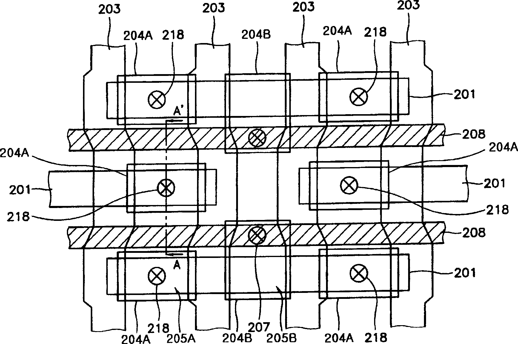
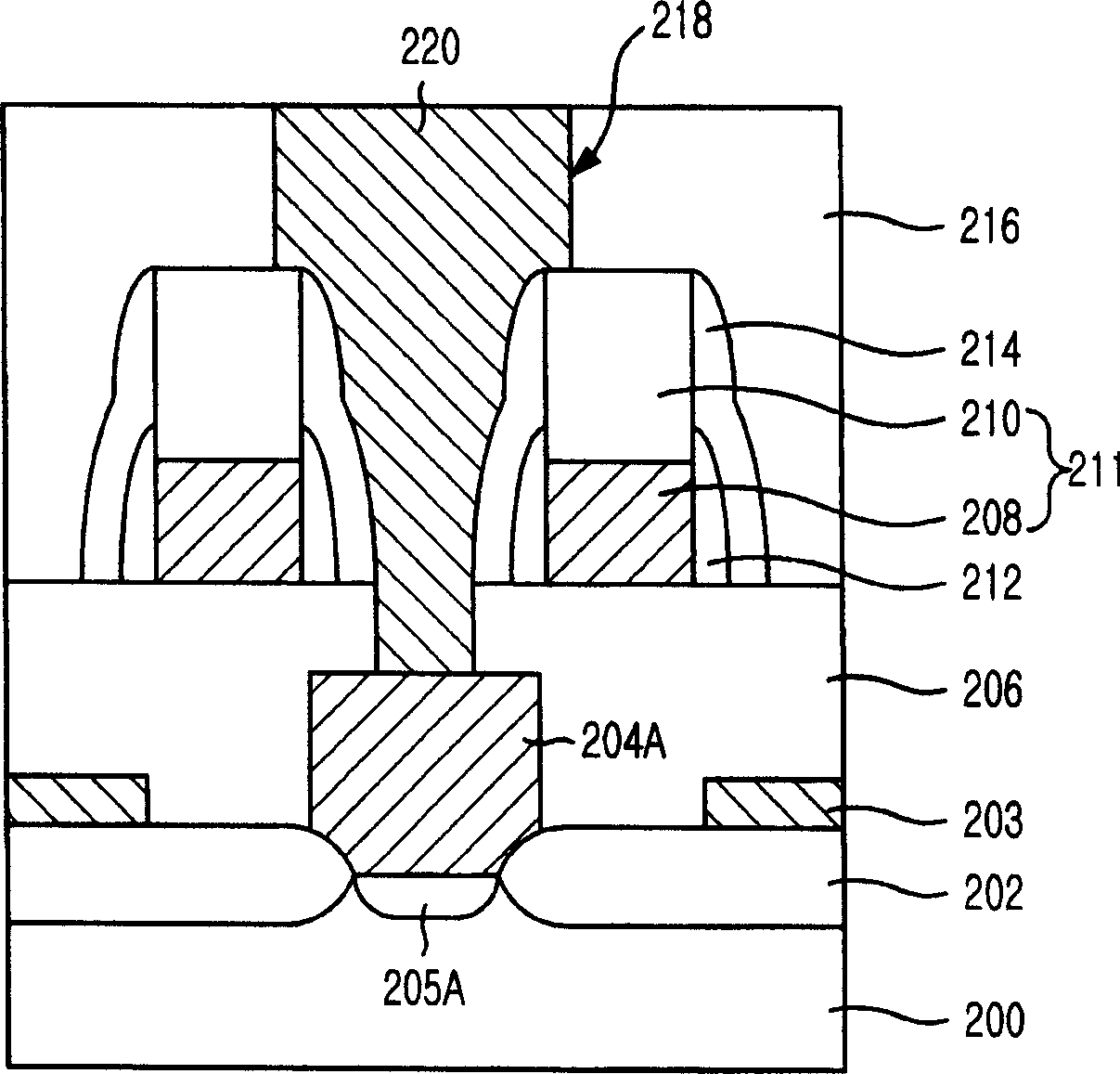
[0054] figure 2 A cross-sectional view of a semiconductor device applied according to a preferred embodiment of the present invention, in particular, a memory cell region is shown in figure 2 middle. image 3 for figure 2 A cross-sectional view along the direction A-A' in FIG. 1 illustrates a semiconductor device with a self-aligned contact (SAC) structure according to a preferred embodiment of the present invention.

[0055] refer to figure 2 and image 3 , a transistor comprising a gate 203 provided to a word line, a capacitive contact region such as a source region 205A and a bit line contact region such as a drain region 205B is formed on a semiconducting substrate 200 . Here, the semiconductor substrate 200 is divided into an active region 201 and a device...


PUM


Abstract

The present invention provides a method for producing semi-conductor. The inventive method includes the steps of: forming a plurality of patterns on a substrate, wherein the patterns are formed by stacking and patterning a first conductive layer, a silicon nitride mask layer and a metal mask layer on the substrate; depositing a first silicon oxide layer along the profile containing the patterns; etching the first silicon oxide layer for forming a silicon oxide spacer with a height lower than a top part of the silicon nitride mask layer so as to partially expose a top part of lateral sides of patterns and simultaneously etching the metal mask layer to expose the silicon nitride mask layer, wherein the metal mask layer prevents losses of the silicon nitride mask layer; forming a silicon nitride spacer on a surface of the silicon oxide spacer and the lateral sides of the patterns; forming a second silicon oxide layer on an entire structure in which the silicon nitride spacer is formed; etching selectively the second silicon oxide layer to expose silicon nitride layer spacer and forming a self-align contact hole that is partially expanded to the top portion of the patterns; and forming a self-align contact structure by filling the self-align contact hole with a second conductive layer.

Description

technical field [0001] The invention relates to a method for manufacturing a semiconductor device; in particular, a method for reducing the parasitic capacitance of a semiconductor storage unit. Background technique [0002] As the integration level of semiconductor devices increases, it is more difficult to achieve the overlay accuracy and process tolerance of the pattern forming process by using a photoregistry. Therefore, a self-aligned contact (hereinafter referred to as SAC) process is particularly adopted and suitable for solving this problem. The SAC process is an etching process that etches objects by using the previously deposited material itself rather than an applied mask. Because of this feature, the SAC process can significantly reduce the cost of manufacturing semiconductor devices. The SAC process itself uses several methods to achieve efficient etching, and among these various methods, a nitride layer is typically used as an etch stop layer. [0003] There...

Claims


Application Information

Patent Timeline
IPC IPC(8): H01L21/336H01L21/027H01L21/28H01L21/60H01L21/768H01L21/82H01L21/8238H01L21/8242
CPCH01L21/76897H01L27/10885H01L27/10855H10B12/0335H10B12/482H01L21/18
Inventor 李圣权金东锡
Owner SK HYNIX INC
Why Eureka
Try Eureka