Method for preparing high-temperature superconducting material intrinsic junction
A superconducting material, high temperature technology, applied in the use of superconducting elements, the manufacture/processing of superconducting devices, and devices containing a junction of different materials, etc., can solve the problem of low repeatability, etc., to achieve the effect of precise control
- Summary
- Abstract
- Description
- Claims
- Application Information
AI Technical Summary
Problems solved by technology
Method used
Image

Examples
Embodiment Construction
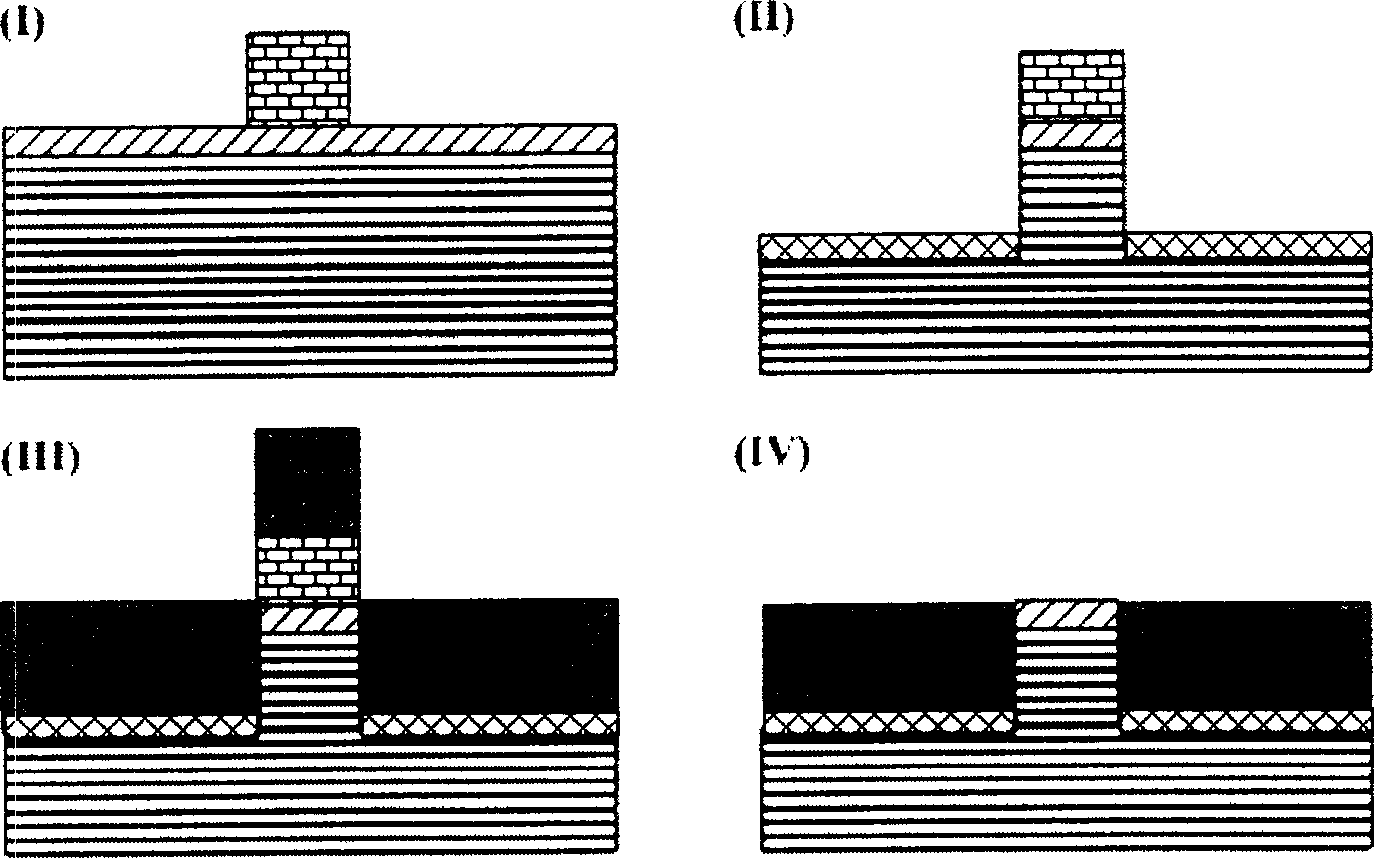
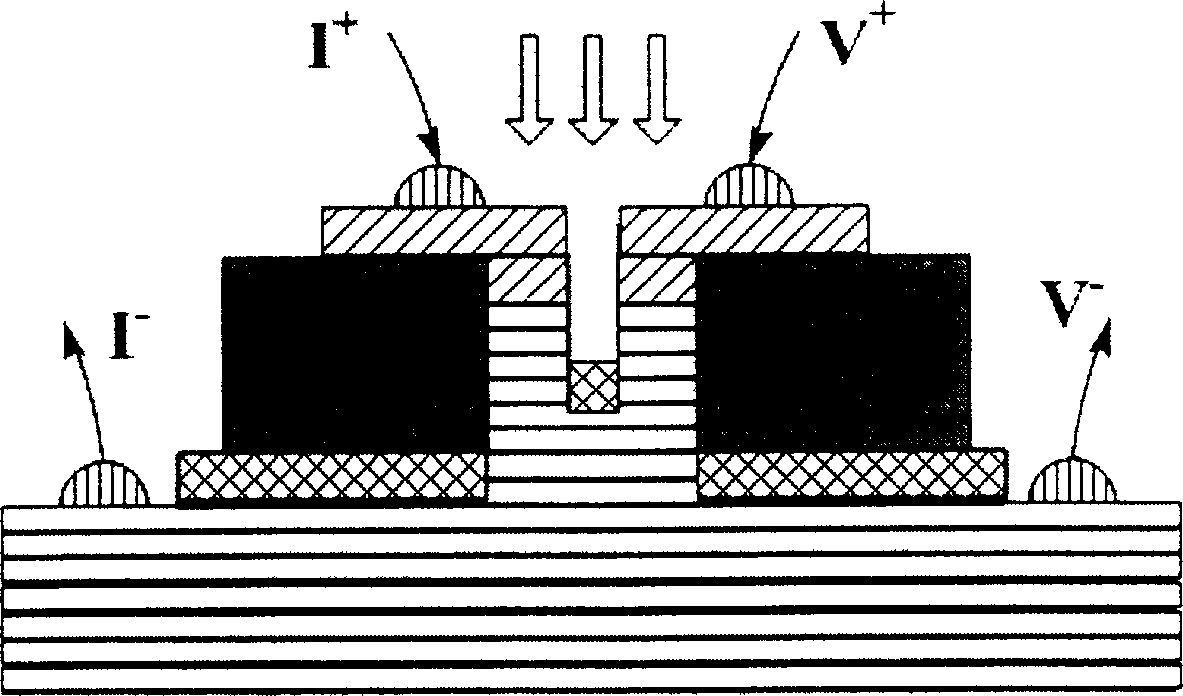
[0021] 1. Using Bi 2 Sr 2 CaCu 2 o 8+x (BSCCO) is a high-temperature superconducting material, the thickness of a single intrinsic junction is 1.54 nanometers, the metal layer material is silver, and the insulating layer material is calcium fluoride.
[0022] ion energy
ER Bi
ER Ag
ER Au
high energy etching
1000eV
0.76mA / cm 2
18nm / min
76nm / min
54nm / min
low energy etch
250eV
0.38mA / cm 2
1.3nm / min
9.3nm / min
6.3nm / min
[0023] ER Bi 、ER Ag and ER Au represent the etch rates of BSCCO, silver and gold, respectively
[0024] The present invention designs and constructs an intrinsic junction containing three junctions. In the experiment, the thickness of the first silver film was 56 nanometers, and the first ion etching time was 12 minutes. The number of junctions in the obtained mesa structure was 7, one more than the expected result. In order to obtain an intrinsic...
PUM
 Abstract
Description
Claims
Application Information
 - Generate Ideas
- Intellectual Property
- Life Sciences
- Materials
- Tech Scout
- Unparalleled Data Quality
- Higher Quality Content
- 60% Fewer Hallucinations
Browse by: Latest US Patents, China's latest patents, Technical Efficacy Thesaurus, Application Domain, Technology Topic, Popular Technical Reports.
© 2025 PatSnap. All rights reserved.Legal|Privacy policy|Modern Slavery Act Transparency Statement|Sitemap|About US| Contact US: help@patsnap.com