

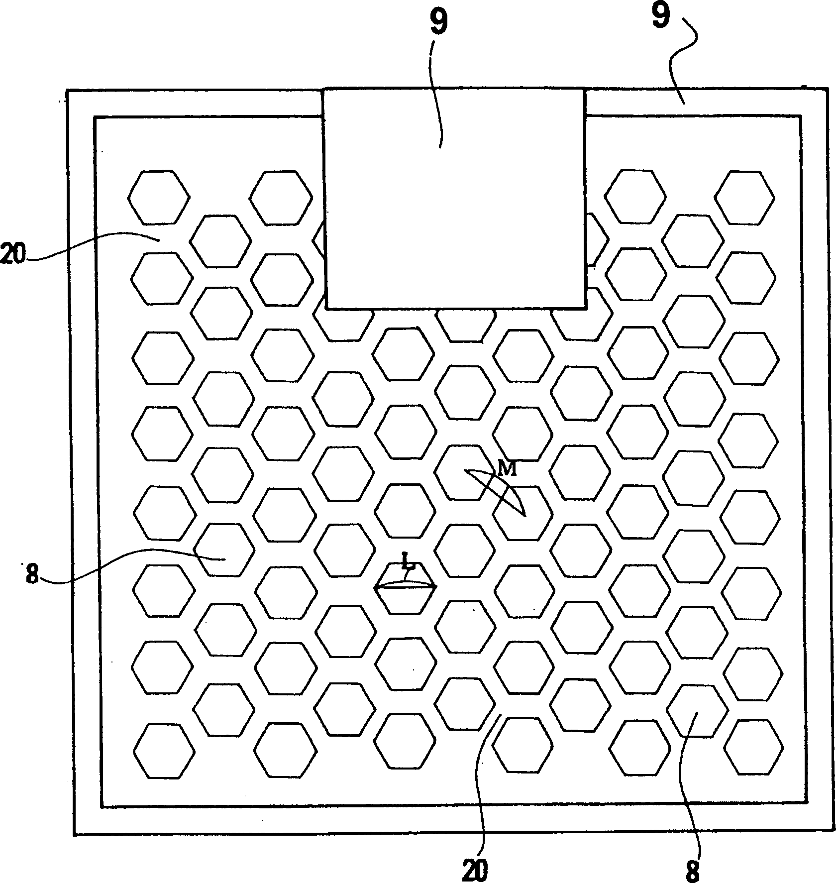
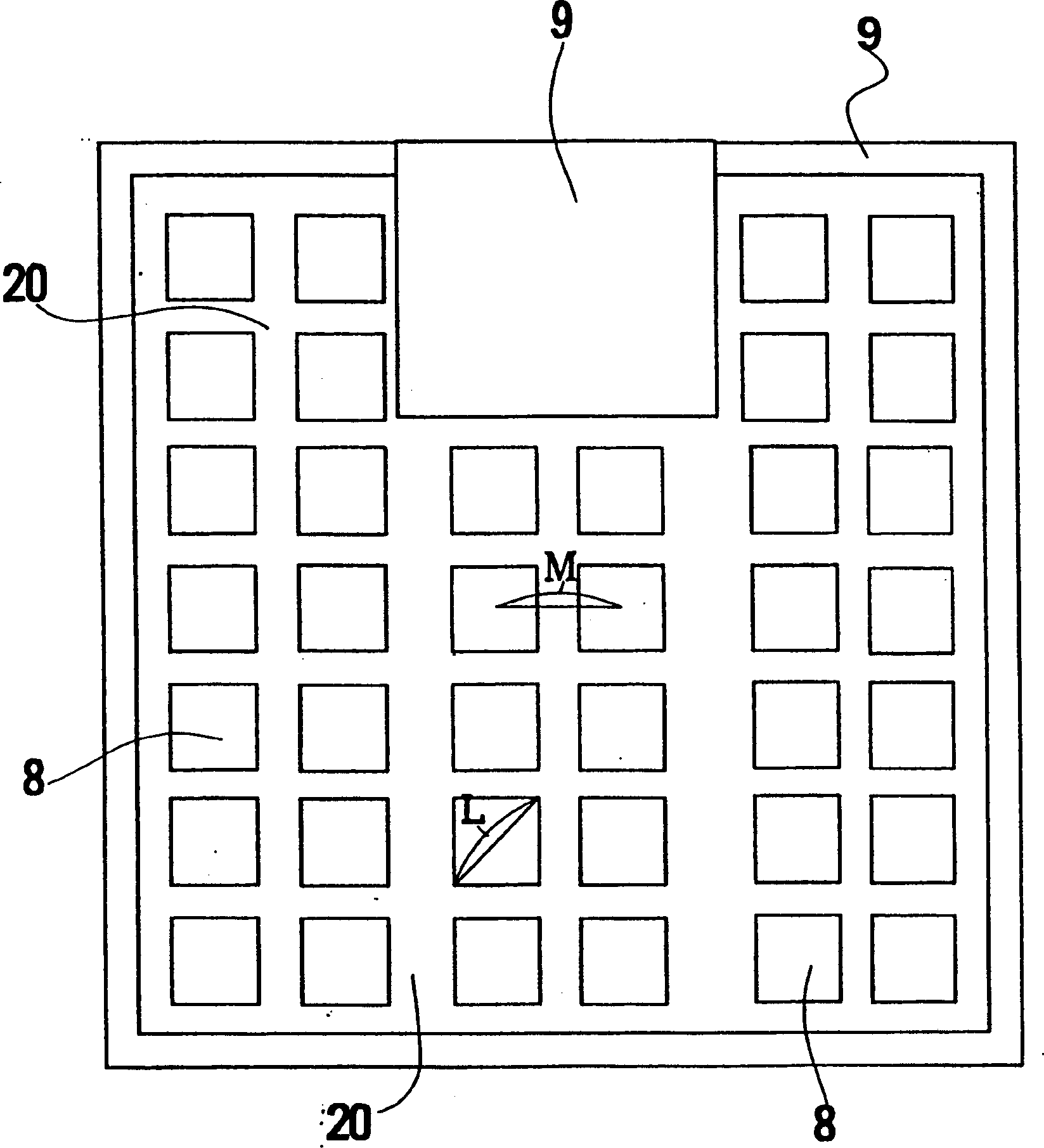
P electrode structure on light exit side of LED
A technology of light-emitting diode and electrode structure, which is applied to circuits, electrical components, semiconductor devices, etc., and can solve problems such as inability to implement low-voltage driving.
- Summary
- Abstract
- Description
- Claims
- Application Information
AI Technical Summary
Problems solved by technology
Method used
Image

Examples
Embodiment Construction
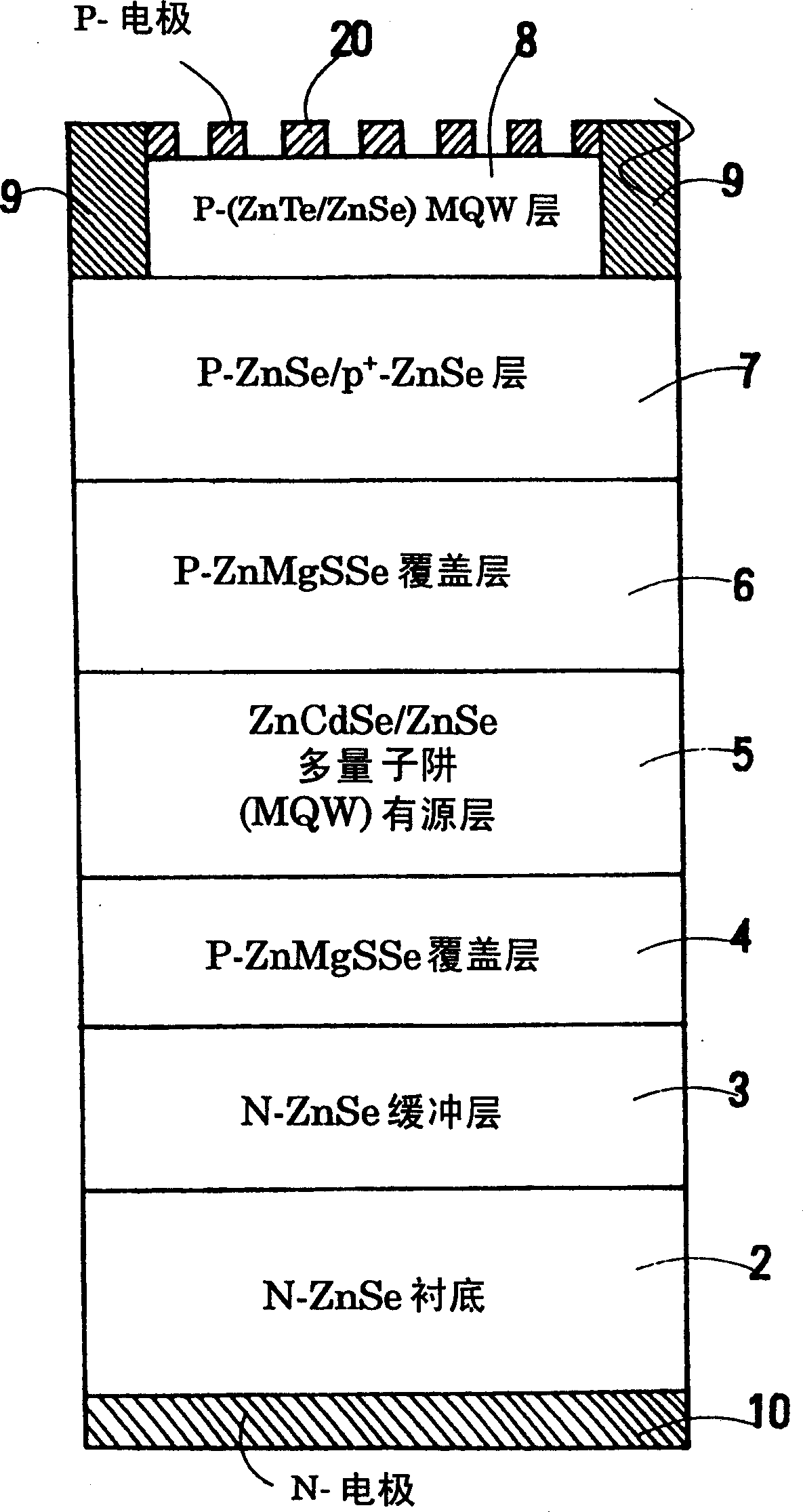
[0110] Specific embodiments of the present invention will be described below with reference to the drawings. The same numerals or symbols in each figure denote the same components to avoid repeated explanations. The dimensional ratios in the drawings do not necessarily agree with those described. [a. Material of light-emitting element]
[0111] The present invention aims to improve LEDs using ZnSe or GaN, which have a wide bandgap and exhibit high resistivity even when deposited with impurities due to the lack of charge carriers. [b. Shape of electrode]
[0112] The present invention aims to improve the shape of the p-electrode from which light emerges. [c.p-type contact layer]
[0113] With wide bandgap semiconductors such as ZnSe or GaN, p-type impurities are not easily deposited. Even when deposition is achieved satisfactorily, the activity ratio is low, and in many cases, not many positive holes are excited from the acceptor. Therefore, the number of p-type carriers ...
PUM
 Abstract
Description
Claims
Application Information