Check patentability & draft patents in minutes with Patsnap Eureka AI!

Interlayer arrangement structure for multilayer circuit board

A technology of multi-layer circuit board and configuration structure, applied in the direction of multi-layer circuit manufacturing, printed circuit, electrical components, etc., can solve the problem of inability to meet high-frequency signal requirements, inability to provide connection between power supply layers and operating components, and the density of via holes. restrictions, etc.

Inactive Publication Date: 2004-02-04
VIA TECH INC
View PDF0 Cites 3 Cited by
  • Summary
  • Abstract
  • Description
  • Claims
  • Application Information

AI Technical Summary

Problems solved by technology

[0005] With the increasing complexity of integrated circuits, the operating frequency is gradually increasing, and the method of cutting the power layer to form the power layout area cannot meet the needs of high-frequency signals
For example, due to the limitation of the area of ​​the power plane after cutting, it is often impossible to provide current in real time during high-speed operation. Therefore, considerable ground / bounce (Ground / Bounce) effects will occur on the power plane, resulting in the entire high-frequency The instability of the signal, and thus make the whole system unable to operate normally
On the other hand, because the density of via holes is getting higher and higher, however, the span (Pitch, such as the distance between two signal lines) of adjacent wiring has its physical limit and must not be too small (generally speaking, within the chip The distance between them is about 3-5mils), so the setting density of via holes is limited
Too few via holes may not provide sufficient connection between the power plane and the operating components, thus making the operating current more unstable

Method used


Image

  • Interlayer arrangement structure for multilayer circuit board
  • Interlayer arrangement structure for multilayer circuit board
  • Interlayer arrangement structure for multilayer circuit board

Examples


Embodiment Construction

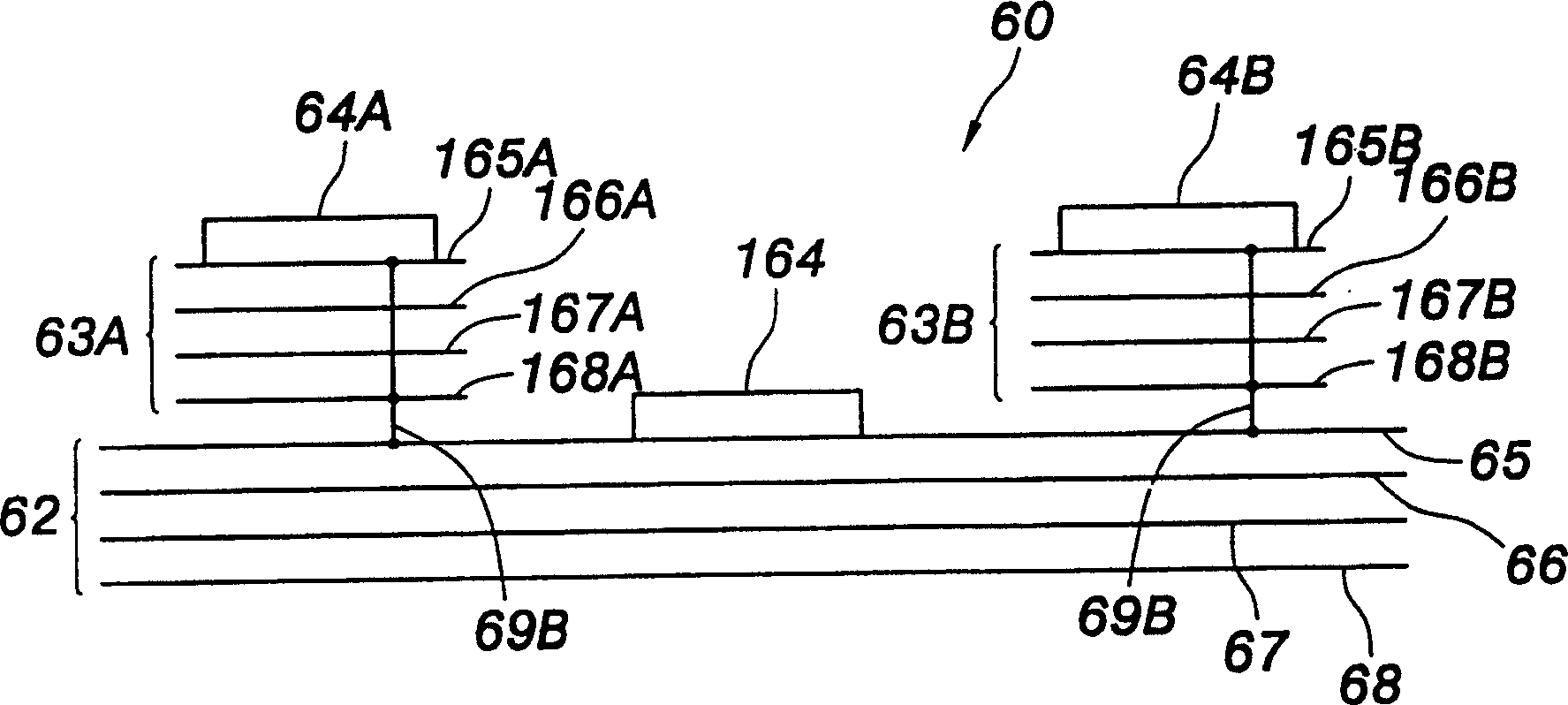
[0018] First see Figure 3A , Figure 3B and Figure 3C , which are schematic plan views of the power supply layer 100 , the component layer 200 , and the soldering layer 300 in the preferred embodiment of the present invention, respectively. Since the ground layer is made of uncut copper foil and is electrically connected to the ground potential, it will not be described in detail. Figure 3A The power supply layer 100 is also basically composed of copper foil, but is cut into several power supply planes 102, 103, 104 and 105, 106 that can provide working voltage, and a reference ground 107 connected to the ground potential. , 108 and 109, wherein the power blocks 102, 103, 104, 105, 106, and the reference grounding areas 107, 108, 109 are isolated from each other by an isolation line 111 to prevent mutual interference. The setting positions of the reference ground areas 107, 108, and 109 correspond to the signal layout areas on the solder layer 300 (in the Figure 3B and...


PUM


Abstract

The present invention relates to an interlayer configuration structure of a multi-layer circuit board. In a preferred embodiment, the circuit board has the structure of four layers from up to down, that is, the component layer, the grounding layer, the power supply layer and the soldering layer, the power supply layer is cut into plural reference grounding areas, the position of each corresponding to the signal distributing area in the soldering layer, so that the signal line distributed in the component layer and the signal line distributed in the soldering layer can refer to the reference ground in the adjacent connecting layer. The power supply layer of the preferred embodiment includes plural power planes which can provide different working voltages.

Description

technical field [0001] The invention relates to an interlayer configuration structure of a multi-layer circuit board, in particular to a reference grounding area cut out in a power supply layer, so that the signal layout area of ​​the soldering layer can also be referred to the power supply layer adjacent to the soldering layer. The reference ground area of ​​the solder layer can be used to make the transmission quality of the signal line of the solder layer to be the same as that of the component layer. Background technique [0002] In recent years, the four-layer stack structure has gradually replaced the printed circuit board with the six-layer stack structure, and has become the most widely used structure. Basically, the four-layer stack structure is arranged from top to bottom into a component layer, a ground layer, a power layer, and a solder layer. The component layer is mainly used for Many integrated circuits and most of the signal lines are laid out, and the groun...

Claims


Application Information

Patent Timeline
IPC IPC(8): H05K1/00H05K3/46
Inventor 陈俊宏陈秀姿陈彦臻
Owner VIA TECH INC
Features
  • R&D
  • Intellectual Property
  • Life Sciences
  • Materials
  • Tech Scout
  • Unparalleled Data Quality
  • Higher Quality Content
  • 60% Fewer Hallucinations
Learn More