Purging method of semiconductor-manufacturing apparatus and manufacturing method of semiconductor device

A technology for a manufacturing device and a manufacturing method, which is applied to the field of purification technology after dry cleaning of a CVD device, can solve the problems of reduced productivity and insufficient purification, and achieves the effects of improving the operation rate, shortening the purification time, and improving the purification efficiency.

Inactive Publication Date: 2004-02-04
KK TOSHIBA
View PDF1 Cites 13 Cited by
  • Summary
  • Abstract
  • Description
  • Claims
  • Application Information

AI Technical Summary

Problems solved by technology

[0004] However, ClF 3 Corrosive gases such as etc. contain halogens with high electronegative properties. For this reason, the corrosive gases adhering to the surface of the reaction chamber cannot be sufficiently detached by short-term purification. As a result, long-term purification was conventionally required.
[0005] If it is a CVD method that can clean the reaction chamber at a low frequency, the long cleaning time after cleaning will not be a particular problem, but in the case of a CVD method that requires cleaning every time a CVD process is performed, it will be reduce productivity

Method used


Image

  • Purging method of semiconductor-manufacturing apparatus and manufacturing method of semiconductor device
  • Purging method of semiconductor-manufacturing apparatus and manufacturing method of semiconductor device
  • Purging method of semiconductor-manufacturing apparatus and manufacturing method of semiconductor device

Examples


Embodiment Construction

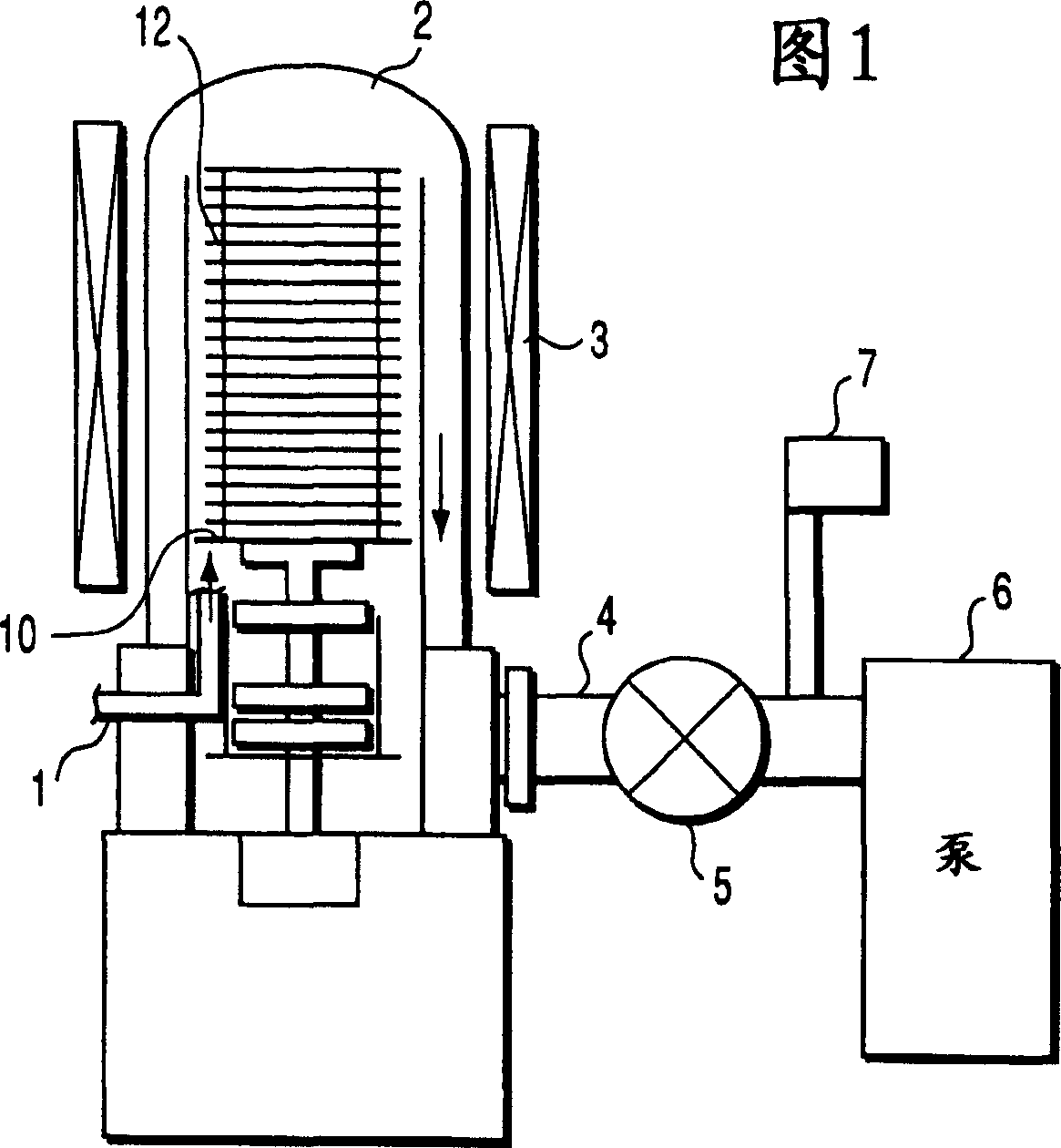
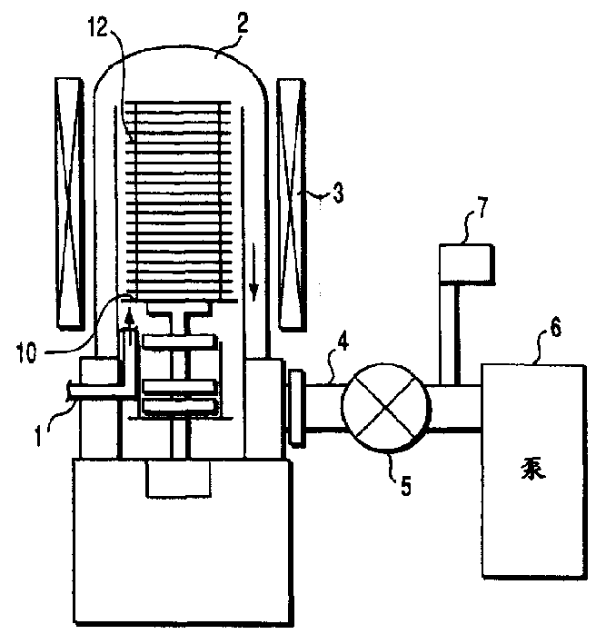
[0017] Referring to Fig. 1, Embodiment 1 will be described.

[0018] FIG. 1 is a schematic cross-sectional view of a vertical CVD apparatus as a semiconductor manufacturing apparatus. A boat 10 is provided in the vertical reaction chamber 2, and a semiconductor wafer 12 such as silicon is placed on the boat before the CVD process. In the lower part of the reaction chamber 2, a gas introduction port 1 is provided. From here, purge gas can be introduced into the interior of the reaction chamber 2 by operation of a mass flow control valve (not shown). A heater 3 is provided outside the reaction chamber 2 in order to heat the semiconductor wafer on the boat 10 in the reaction chamber 2 . A pump 6 is connected to the reaction chamber 2 through an exhaust pipe 4 having a pressure control valve 5, by operation of which the inside can be properly exhausted.

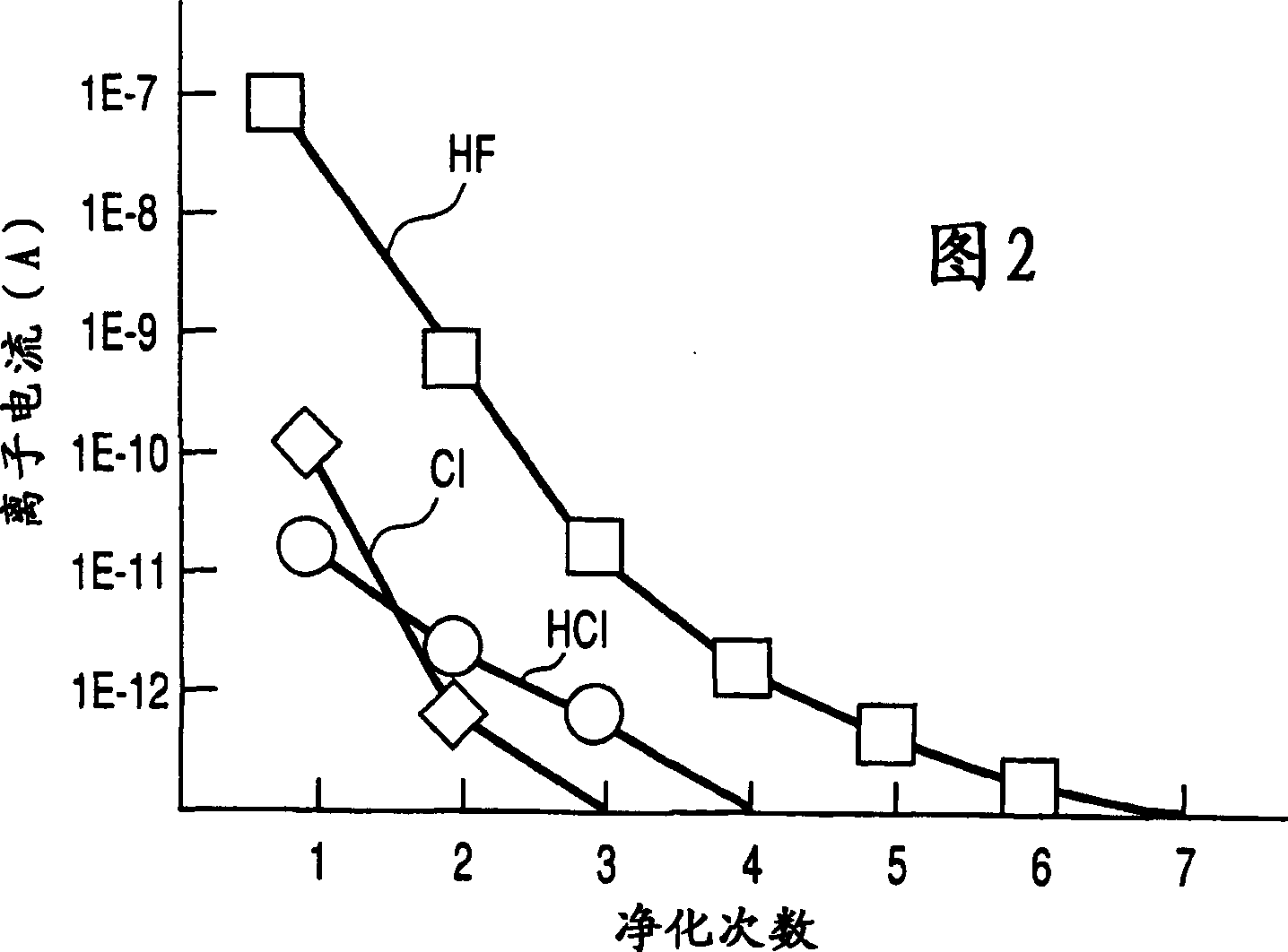
[0019] Using the CVD apparatus shown in FIG. 1, on the semiconductor wafer 12 on the boat 10, after forming a silicon film b...


PUM


Abstract

A method of purging a semiconductor manufacturing apparatus comprises a step of etching a CVD-deposited film deposited in a chamber (2) constituting a semiconductor manufacturing apparatus which has performed a process of forming a CVD film using a CVD process over a semiconductor wafer (12) by using an etching gas containing at least a halogen gas, and a step of purging a cleaning gas remaining in the chamber (2) by causing a gas containing hydrogen to flow into the chamber (2) after the step of etching the CVD-deposited film by using the cleaning gas.

Description

technical field [0001] The invention relates to a purification process of a semiconductor manufacturing device, in particular to a purification process after dry cleaning of a CVD (Chemical Vapor Deposition) device. Background technique [0002] Semiconductor manufacturing equipment, such as CVD equipment such as LP (low pressure)-CVD, will deposit silicon, silicon oxide, silicon nitride in its reaction tank (hereinafter referred to as the reaction chamber) or use it in semiconductor devices. other film materials. When such a CVD-deposited film becomes too thick, there is a problem of contamination in the reaction chamber due to film peeling. In addition, when the film thickness of the deposited film in the reaction chamber becomes non-uniform due to film peeling, there is another problem that it is difficult to uniformly form the CVD film to be formed on the semiconductor wafer. Therefore, in the past, before such problems became significant, it was resorted to using ClF ...

Claims


Application Information

Patent Timeline
Patent Type & Authority Applications(China)
IPC IPC(8): C23C16/44H01L21/205
CPCY10S438/905C23C16/4412C23C16/4408C23C16/4405H01L21/205
Inventor 水岛一郎
Owner KK TOSHIBA
Why Eureka
Try Eureka