Cross mark transport method, cross mark transport device and exposure device

A technology for cross mark and handling device, which is applied in the direction of exposure device, printing device, transportation and packaging of photoplate making process, and can solve the problems of unable to maintain the cross mark substrate

Inactive Publication Date: 2004-02-11
NIKON CORP +1
View PDF0 Cites 9 Cited by
  • Summary
  • Abstract
  • Description
  • Claims
  • Application Information

AI Technical Summary

Problems solved by technology

[0004] However, the conventional cross-mark transfer device cannot hold such a thin round cross-mark substrate

Method used


Image

  • Cross mark transport method, cross mark transport device and exposure device
  • Cross mark transport method, cross mark transport device and exposure device
  • Cross mark transport method, cross mark transport device and exposure device

Examples


Embodiment Construction

[0069] Next, the embodiments of the present invention will be described with reference to the drawings.

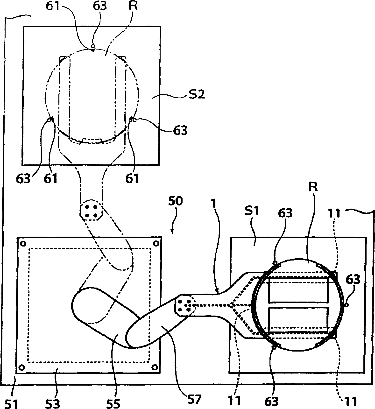
[0070] figure 2 It is a plan view of the overall structure of the cross mark conveying device according to the embodiment of the present invention.

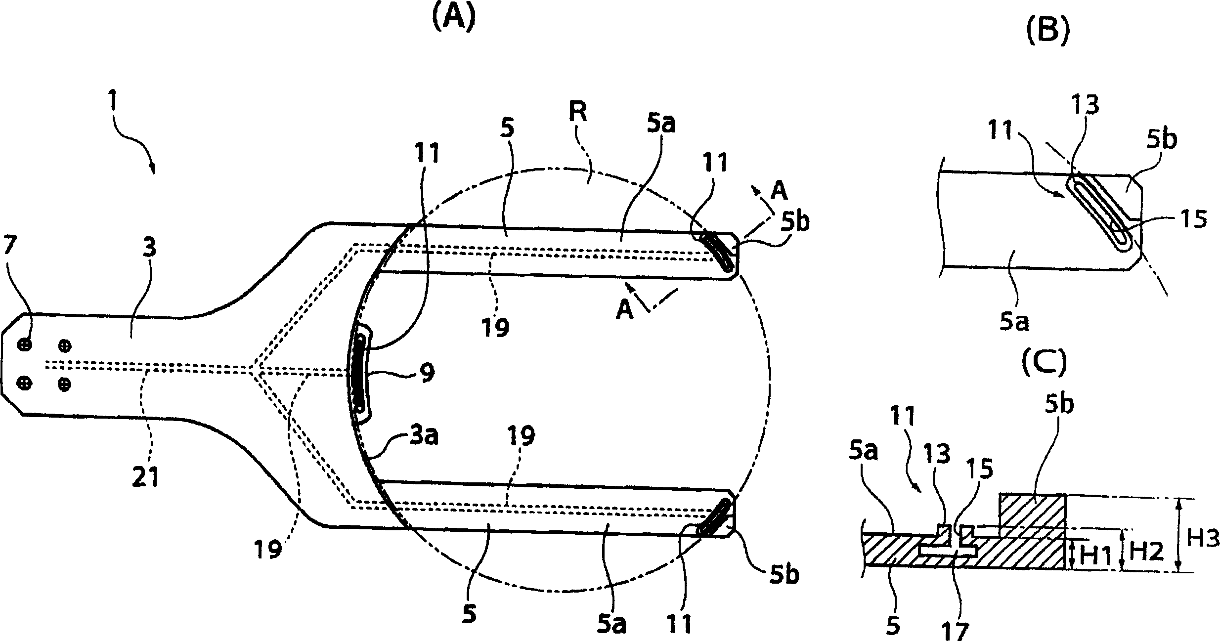
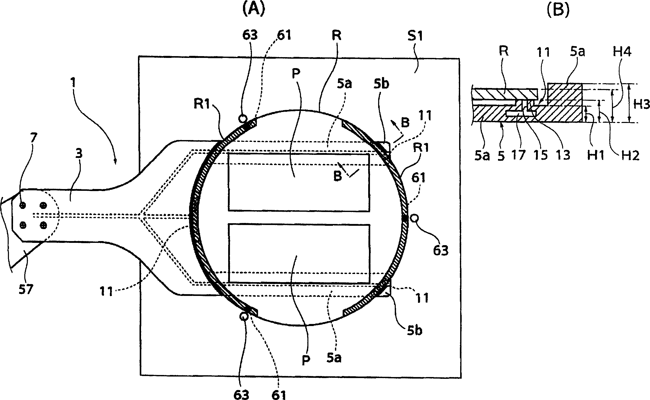
[0071] Figure 3A is a diagram showing figure 2 An enlarged view of part of the cross marking handling device. FIG. 3B is a cross-sectional view along line B-B of FIG. 3A.

[0072] first reference figure 2 The overall structure of the cross mark transfer device will be described.

[0073] The cross conveyance device 50 conveys the cross R between two workstations (stations) S1 and S2 in the atmosphere. The workstation can be, for example, a reticle pot, a pre-aligner chamber, or a load-lock chamber, among others. This mechanical arm (cross mark carrying device) 50 comprises the base 53 that is fixed on the stand 51; The first arm 55 that is rotatably installed on the base 53; the second arm 57 ; and a U-shaped hook (...


PUM


Abstract

Robotic reticle manipulators are disclosed for use in holding and conveying, with good stability, thin, circular reticles as used in charged-particle-beam ( e.g. , electron-beam) microlithography. An embodiment of such a manipulator includes at least one arm configured for executing movements in the X-, Y-, and Z-directions. Connected to the distal end of the at least one arm is a U-shaped fork (as an exemplary reticle-support member) defining recessed surfaces and vacuum ports for holding the reticle at the reticle's narrow handling zone located along the periphery of the reticle. Each vacuum port includes an upwardly extending lip that defines, on its "upward"-facing surface, a respective reticle-contact surface. Three such vacuum ports are provided on the fork and are situated so as to be nearly equidistantly separated from one another. Thus, as the reticle is being held and conveyed by the manipulator, the reticle is securely held to prevent reticle damage.

Description

technical field [0001] The present invention relates to a reticle handling method and a handling device used as a pattern original plate of a semiconductor exposure device. Background technique [0002] Conventional semiconductor exposure devices use i-line, KrF, ArF, etc. as light sources. The cross marks used in these exposure devices are made of glass, have a square shape, and have a thickness of several millimeters. Generally, most of the common cross mark processing devices correspond to this kind of cross mark. [0003] In recent years, the development of an exposure apparatus using an electron beam (EB) has been progressing as an exposure apparatus capable of achieving both high resolution and high productivity. This EB exposure apparatus does not use the conventional glass square cross mark, but uses a thin circular cross mark of the same shape as SEMI standard wafers and SEMI standard V-shaped mark wafers (notch wafers). The thickness of the cross mark is about 0...

Claims


Application Information

Patent Timeline
Patent Type & Authority Applications(China)
IPC IPC(8): H01L21/677G03B27/62G03F7/20H01L21/027
CPCB82Y10/00Y10S414/136Y10S414/141B82Y40/00H01J37/3174Y10S414/135H01L21/67766G03B27/62H01L21/68707G03F7/70741Y10S414/14H01L21/027
Inventor 菊地秀和山本明宏
Owner NIKON CORP
Why Eureka
Try Eureka