Packaging baseplate having electrostatic discharge protection

A technology for electrostatic discharge protection and packaging substrates, applied in circuits, electrical components, electrical solid devices, etc., can solve problems such as failure of packaging products, chip damage, and static electricity generation, so as to improve the good rate and protect from electrostatic charge damage. Effect

Inactive Publication Date: 2004-03-03
ASE SHANGHAI
View PDF0 Cites 8 Cited by
  • Summary
  • Abstract
  • Description
  • Claims
  • Application Information

AI Technical Summary

Problems solved by technology

Most chips do not have this ESD protection circuit design
[0003] In addition, during the process of chip encapsulation or sealing, due to the process of injecting the sealant into the chip, when the sealant rubs,

Method used


Image

  • Packaging baseplate having electrostatic discharge protection
  • Packaging baseplate having electrostatic discharge protection
  • Packaging baseplate having electrostatic discharge protection

Examples


Embodiment Construction

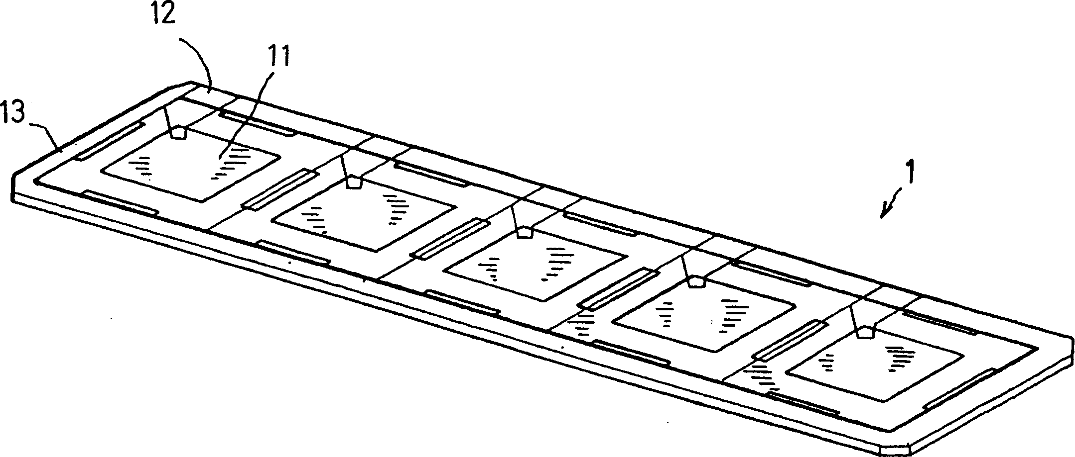
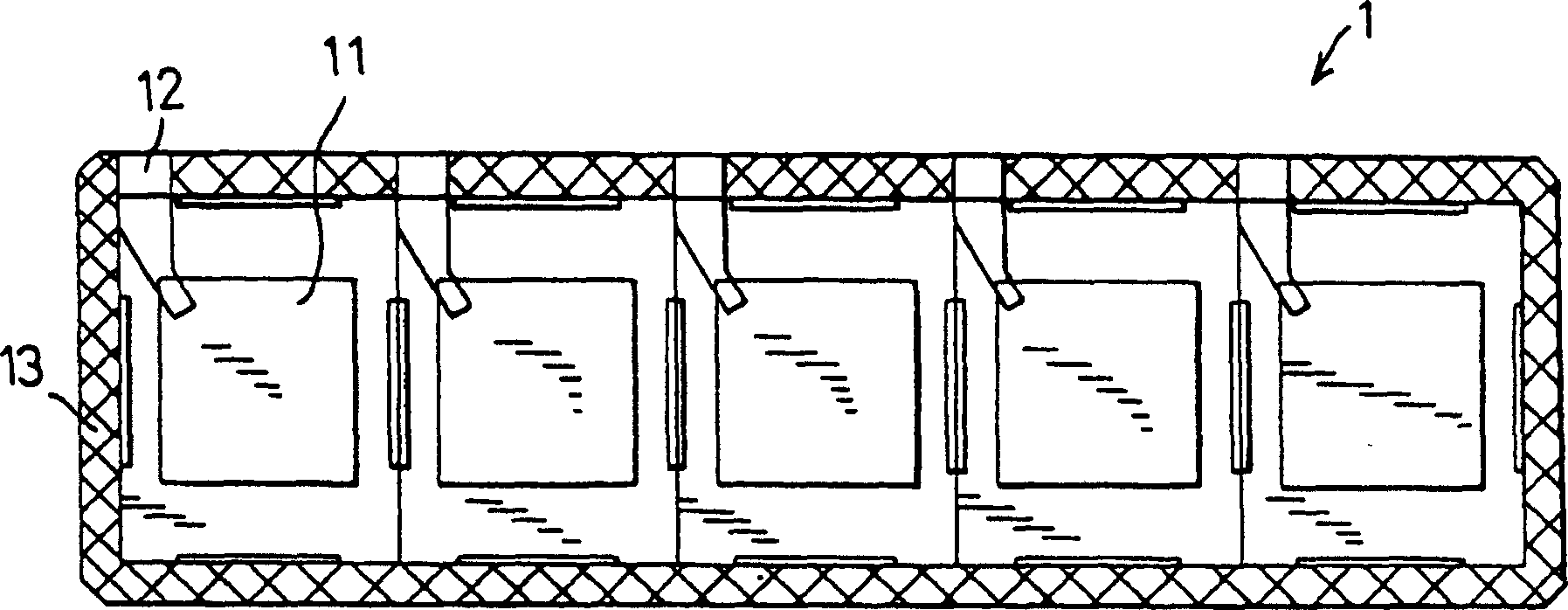
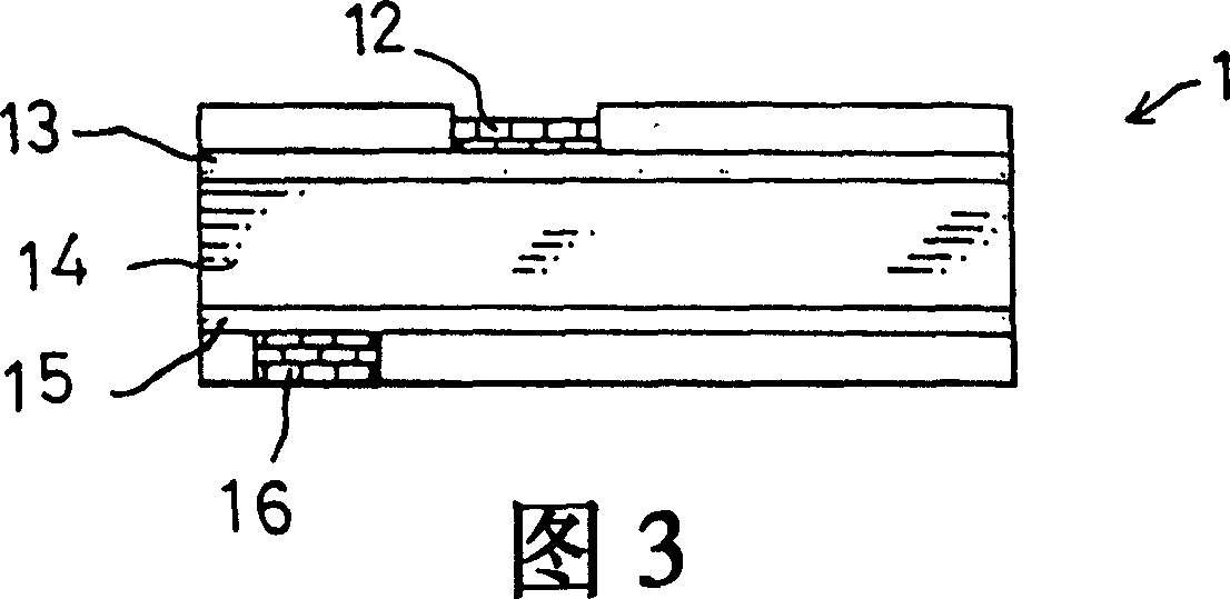
[0029] refer to figure 1 , figure 2 And Fig. 3, the packaging substrate 1 with electrostatic discharge protection of the first embodiment of the present invention comprises: five chip holders 11, five injection molding ports 12, a first copper mesh layer 13, a dielectric layer 14, a second Copper mesh layer 15 and a metal pad 16 . The chip holder 11 is used to carry the chip to be packaged. Each injection molding port 12 is connected to each die holder 11 by the edge of the packaging substrate 1 , and is used for guiding the encapsulant to inject into each die holder 11 . The injection molding ports 12 are disposed on the top surface of the packaging substrate 1 . The metal pad 16 is disposed on the bottom surface of the packaging substrate 1 .

[0030] The first copper mesh layer 13 is disposed on the periphery of the packaging substrate 1 , and the first copper mesh layer 13 is electrically connected to each injection molding port 12 at the periphery of the packaging su...


PUM


Abstract

Each die-casting orifice of package base plate is connected to first copper wire mesh layer electrical. The copper wire mesh is positioned at periphery of top surface of package base plate. Static charge generated in procedure of package chips is leaded to first copper wire mesh layer through die casting orifice. The static charge is gathered and confined at capacitance composed of first copper wire mesh layer, dielectric layer and second copper wire mesh layer. Or using a through hole connected to first and second copper wire mesh layers through metal pads and bearing object lead static charge out. Thus, by using capacity effect or conductive effect, the static charge is leaded out so as to raise qualified rate.

Description

technical field [0001] The invention relates to a package substrate, in particular, the invention relates to a package substrate with electrostatic discharge protection. Background technique [0002] Integrated circuits typically operate at 5 volts or less, and when an integrated circuit is subjected to higher voltages, it usually damages the integrated circuit. For the static electricity generated by friction, induction, contact, etc., only a few of the existing chips have an electrostatic protection circuit design inside to protect the chip from damage caused by static electricity. Most chips do not have this ESD protection circuit design. [0003] In addition, during the process of chip encapsulation or sealing, due to the process of injecting the sealant into the chip, when the sealant rubs, senses, or contacts with the substrate or other media, static electricity may be generated, and the damage of this electrostatic discharge will make the chip Failure damage, result...

Claims


Application Information

Patent Timeline
IPC IPC(8): H01L23/12H01L23/60
Inventor 蒋荣生
Owner ASE SHANGHAI
Why Eureka
Try Eureka